

The last decade has seen the discovery of many materials with extraordinary electronic properties reflecting original quantum effects induced by their dimensionality and topology. Following the example of the physical effects found in graphene, can these properties be induced in semiconductor materials, the main components of the microelectronics industry? This is what IEMN researchers have just shown, in collaboration with colleagues from Utrecht, Shanghai, Bordeaux and Paris-Saclay, thanks to innovative nanotechnological approaches on III-V semiconductors.
When a crystal is reduced to two dimensions, electrons have totally unusual and counterintuitive quantum properties. In some materials such as graphene, electrons can behave as relativistic massless particles, much like photons. On the other hand, in other materials, electrons can be placed in totally flat electronic strips, giving them an infinite mass. These flat-band electronic systems are currently attracting considerable interest from physicists. Indeed, since electrons have zero kinetic energy, very original quantum phases can be formed, for example superfluid phases.
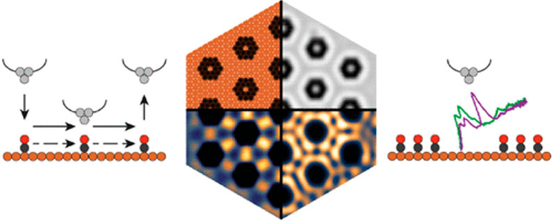
Can these effects be induced in artificial materials, whose properties would result from their manufacture and thus from electronic band engineering? This is the question that researchers from the IEMN and the Debye Institute in Utrecht have addressed. The track explored is to start from a medium in which electrons are originally perfectly free to move in two dimensions. Thanks to the application of a periodic potential, the electron waves are scattered by the potential, inducing the desired band dispersions under the effect of quantum interference. This approach requires to structure the free electron gas with a periodicity close to the electron wavelength, from a few nanometers to a few tens of nanometers depending on the chosen materials. It has been recently validated in Utrecht, in collaboration with the IEMN, in the case of electrons localized on a copper surface subjected to a periodic array of CO molecules displaced by means of a tunneling tip [1].
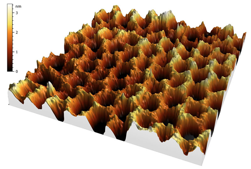
Inducing these same effects in a conventional semiconductor, such as those used by the microelectronics industry, would obviously open up fascinating prospects for integratable quantum platforms compatible with microelectronic technologies. A first step towards this goal has just been taken and published in the journal Nano Letters [2]. A honeycomb lattice has been fabricated in an InGaAs quantum well using an original nanostructuring technique developed at the LCPO in Bordeaux, the block copolymer lithography which allows to reach lattice parameters of the order of 21 nm. Tunneling spectroscopy measurements performed at IEMN and Utrecht demonstrate a profound modification of the electronic band structure, as predicted. In particular, despite the disorder effects inherent to nano-lithography, the spectra have the expected characteristics by the formation of flat bands with a very high density of electronic states. This feat, which required pushing the limits of current lithography techniques, opens the way to the generation of non-trivial quantum phases in the most common semiconductor materials.
Read more
[1] p Orbital Flat Band and Dirac Cone in the Electronic Honeycomb Lattice
T.S. Gardenier, J.J. van den Broeke, J.R. Moes, I. Swart, C. Delerue, M.R. Slot, C. Morais Smith, and D. Vanmaekelbergh. ACS Nano 14 (10), 13638-13644 (2020).
https://dx.doi.org/10.1021/acsnano.0c05747
[2] Engineering a Robust Flat Band in III–V Semiconductor Heterostructures
N.A. Franchina Vergel, L. Christiaan Post, D. Sciacca, M. Berthe, F. Vaurette, Y. Lambert, D. Yarekha, D. Troadec, C. Coinon, G. Fleury, G. Patriarche, T. Xu, L. Desplanque, X. Wallart, D. Vanmaekelbergh, C. Delerue, and B. Grandidier. Nano Letters 21 (1), 680-685 (2021).
https://dx.doi.org/10.1021/acs.nanolett.0c04268
supports ANR : ANR-16-CE24-0007-01 et ANR-17-CE09-0021-03


