


![]()

Ultrafast mid-infrared photodetectors
Thanks to carrier lifetimes of the order of one picosecond, mid-infrared (MIR – λ ~ 3-15μm) photo-detectors based on inter-sub-band transitions in III -V hetero-structures can potentially reach bandwidths of several hundreds of GHz. A team of IEMN researchers, in collaboration with researchers from C2N Laboratory in Paris and the Key Laboratory of Terahertz Science in Shanghai, have exploited this property to demonstrate an ultra-fast MIR photo-detector with a 3dB bandwidth > 70GHz at room temperature, the broadest reported to date at these wavelengths.
The response time of a semiconductor-based photo-detector is determined primarily by two key factors. On the one hand, inside the semiconductor material itself, we have the lifetime of the carriers excited by the incident radiation. This is called the intrinsic response time. On the other hand, the detector is connected to an external electrical circuit, providing so-called parasitic elements or simply parasitics, (capacitance, resistance and / or inductance), which determine the device electrical response time. The challenge is to minimize the parasitic effects in order to achieve the intrinsic response.
Unlike visible or near infrared semiconductor-based detectors, where the electrons lifetime is determined by inter-band recombination processes, in multi-quantum well mid-infrared (MIR) photo-detectors, such as the one demonstrated in this work, electrons occupy levels or mini-bands inside the conduction band. As a result, the photo-excited carriers recombine via the emission of optical phonons, resulting in extremely short lifetimes, on the order of one picosecond. Intrinsic bandwidths of several hundred GHz are therefore potentially achievable.
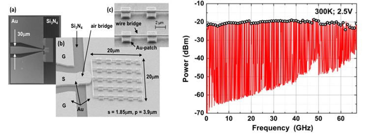
In this work, carried out in the THz Photonics group at IEMN, we exploit a ~350nm thick GaAs/Al0.2Ga0.8As multi-quantum well heterostructure to demonstrate a MIR detector at l ~ 10mm. The device has been entirely fabricated in the IEMN cleanroom facility.
To allow ultrafast operation and illumination at normal incidence, the detector consists of a 50W coplanar waveguide, monolithically integrated with a 2D-array of sub-wavelength patch antennas, electrically interconnected by suspended wires. With this device architecture we obtain a parasitic capacitance of ~30fF, corresponding to the static capacitance of the antennas, yielding a RC-limited 3dB cutoff frequency >150GHz at 300K, extracted with a small-signal equivalent circuit model. Using this model, we quantitively reproduce the detector frequency response and find intrinsic roll-off time constants as low as 1ps at room temperature.
The detector’s frequency response was measured at the IEMN Characterization Center. To this end we have upgraded a 67GHz cryogenic probe station, in order to allow the simultaneous illumination of the detector by two MIR quantum cascade lasers. The resulting heterodyne beat-note, i.e. the ac component of the photocurrent oscillating at the difference frequency between the two lasers, is then detected using a spectrum analyzer. The result of the measurement at room temperature is shown in the figure above (right panel) where each red line represents a heterodyne beat. An almost flat frequency response up to 70 GHz (black circles) is obtained, limited by the measuring system’s bandwidth. This is the largest bandwidth demonstrated to date for a quantum well MIR photo-detector, with, at the same time, state-of-the-art responsivities of 0.15 A / W and 1, 5 A / W respectively at T = 300K and T = 77K. These detectors have many potential applications in areas such as free space communications, military countermeasures, astrophysics, as well as gas detection and high-resolution spectroscopy.


