

14/01/2020
2.00 pm - IEMN Central Laboratory - Amphitheatre
Campus Cité Scientifique – Villeneuve d’AscqDr. Claire Berger,
Georgiatech Metz
Abstract:
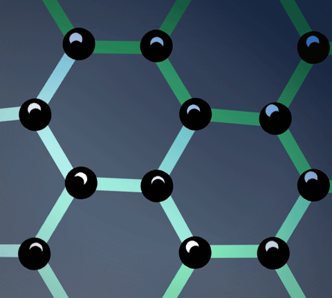
More than two decades of work on carbon nanotubes and more recently on graphene have largely contributed to the idea of carbon-based electronics. Graphene grown epitaxially on silicon carbide (epigraphene) presents the textbook properties of graphene, and can be grown reproducibly and reliably at a very large scale, all the while realizing high quality graphene structures at the nanoscale. Depending on the interaction with the growth substrate, epigraphene sh
ows a range of properties from semiconducting behavior to exceptional conduction. Narrow ribbons grown on facets etched in the SiC substrate show room temperature single channel quantized ballistic conductors on distances greater than 15 µm. Charge neutral, epigraphene grown on these facets gives access to physics at the Dirac-point. Besides their importance for fundamental science, epigraphene nanoribbons are readily produced by the thousands and their room temperature ballistic transport properties are promising for advanced nanoelectronics.
Biography:
- Director of Research at Centre National de la Recherche Scientifique, France
- Professor of the Practice, Georgia Institute of Technology, Atlanta
email: cberger@georgiatech-metz.fr claire.berger@physics.gatech.edu
Education
- University Joseph Fourier, Grenoble - France, PhD, Physics, 1987.
- University Joseph Fourier, Grenoble - France, Habilitation à Diriger des Recherches, 1996.
Appointments and Research Activities
 1988-2001: CNRS Research Fellow (Grenoble):
Transport properties of quasicrystalline and related materials, Quasicrystal growth and structural studies, Metal-insulator transition, quantum interference effects
2001-present: CNRS - Georgia Institute of Technology dual appointment.
2007: CNRS Research Director (Institut Néel, Grenoble)
2017: CNRS-Directeur de Recherches 1ère classe and GT Professor of the Practice
Growth, electronic and structural properties of low dimensional graphite, epitaxial graphene, carbon nanotubes. Low temperature transport.
Five Selected Publications
- Exceptional ballistic transport in epitaxial graphene nanoribbons
J. Baringhaus, M. Ruan , F. Edler, A. Tejeda, M. Sicot, A. Taleb-Ibrahimi, A.P. Li, Z. Jiang, E.H. Conrad, C. Berger, C. Tegenkamp, W. A. de Heer, Nature 506, 349 (2014).
- Large area and structured epitaxial graphene produced by confinement controlled sublimation of silicon carbide. W. A. de Heer, C. Berger, M. Ruan, M. Sprinkle, X. Li, Yike Hu, B. Zhang, J. Hankinson, E.H. Conrad, PNAS 108 (41) 16900 (2011).
- Scalable templated growth of graphene nanoribbons on SiC
M. Sprinkle, M. Ruan, X. Wu, Y. Hu, M. Rubio-Roy, J. Hankinson, C. Berger, W. A. de Heer.
Nature Nanotechnology 5, 727 (2010).
- Electronic confinement and coherence in patterned epitaxial graphene, C Berger, Z. Song, X. Li, X. Wu, N. Brown, C. Naud, D. Mayou, T. Li, J. Hass, A. N. Marchenkov, E. H. Conrad, P. N. First, W. A. de Heer, Science 3012, 1191 (2006).
- Ultrathin epitaxial graphite: 2D electron gas properties and a route toward graphene-based nanoelectronics, C. Berger, Z.Song, T. Li, X. Li, A. Y. Ogbazghi, R. Feng, Z. Dai, T. Grenet, A. N. Marchenkov, E. H. Conrad, P. N. First, W. A. de Heer, J. Phys. Chem. B 108, 19912 (2004).
Selected activities:
- Over 28000 citations; H-index 63; more than 230 research publications; over 70 invited research lectures and conferences.
- Co-chair of 2 international schools and 7 international workshops (Epitaxial graphene 2009, 2010, 2011, France -Atlanta 2011, quasicrystals 1991, 1994, 1998).
- On the Editorial Board of Journal of Physics - Materials. Co-editor of the book: Quasicrystals : current topics (1999) and of the J Phys D epitaxial graphene special topics issue (2012).
- 20 PhD supervised or co-supervised students and 5 post-docs. Over 30 engineering or physics major Master and Undergrad students, REU students, high school teachers interns (training and mentoring for full time summer semester or full year part time).
- Selected outreach activities: public lectures in Atlanta; presentations at middle school science and career days; design and presentation of experiments at seven French national scientific exhibits, CNRS open house events, middle school science and career fairs, interview in 3 French National TV science programs.
Honors and Awards
Thomson-Reuter / Clarivate Analytics Highly cited Researcher 6 years in a row 2014-2019; APS Fellow, 2013; Louis Ancel Prize - Société Française de Physique, 2001; Bronze Medal of CNRS (award for young researchers) 1988.


