IEMN
  • Home
  • News
    • IEMN Newsletters
    • M2-Ingé Internships
    • Job offers
    • All news
  • The Institute
    • Presentation
    • Organization of the institute
    • The Scientific Department
    • The Technological Department
    • Administrative and financial management
    • Rules of procedure
    • Our commitments
  • The Research
    • Scientific departments
      • Nanostructured Materials and Components
      • Micro / nano optoelectronics
      • Telecommunications Technologies and Intelligent Systems
      • Acoustic
    • Research groups
    • Flagship
  • Scientific Production
    • IEMN publications
    • Scientific production resources
  • The platforms
    • CMNF - Central Platform for Micro Nano Manufacturing
      • Engraving and implantation pole
      • In Line Analysis Unit
      • Soft Lithography and Bio Microfluidics
      • Deposits and epitaxy division
      • Lithography Unit
      • Packaging Division
      • CMNF Staff
    • PCMP - Multi-Physics Characterization Platform
      • Scanning Probe Microscopy Facility
      • Hyperfrequency, Optical and Photonic Characterization (CHOP)
      • Advanced Communications Systems and Prototyping cluster (SigmaCOM)
      • Characterisation, ElectroMagnetic Compatibility and Prototyping Centre (C2EM)
      • PCMP Staff
    • Services offered by our platforms
  • Partnership - Valuation
    • Academic Collaborations
    • ANR Projects
    • Main international collaborations
    • Industrial partnerships
    • The joint IEMN-Industry laboratories
    • Startups
  • Research Training
    • After the thesis
      • Do a post-doc at the IEMN
      • Towards the world of business and industry
      • Become a teacher-researcher
      • Become a Researcher
      • Starting a business at IEMN
      • FOCUS on a SATT engineer from the IEMN
    • A thesis at IEMN
      • Thesis and HDR defenses
      • Thesis topics
      • Financing
      • Doctoral studies
    • Master - Engineer
      • Masters ULille
        • Master Life Sciences and Technologies graduate programme
        • Master Nanosciences and Nanotechnologies - Speciality ETECH
        • Master Networks and Telecommunications
      • UPHF-INSA Masters
        • Master in Embedded Systems and Mobile Communications Engineering
        • Master Cyber Defense and Information Security
        • Master in Materials, Control and Safety
        • Master in Image and Sound Systems Engineering
      • Partner/Tutoring Engineering Schools
      • M2-Ingé Internships
    • The Lille branch of the GIP-CNFM
    • Nano-École Lille
  • Contact Us
    • Location
    • Contact form
    • Annuaire Intranet
    • « Suivez-nous »
  • Our support
  • fr_FR
  • Rechercher
  • Menu Menu
NEWS

Journées SCOPe 2019

19-20 June 2019

Paris-Est Institute of Chemistry and Materials

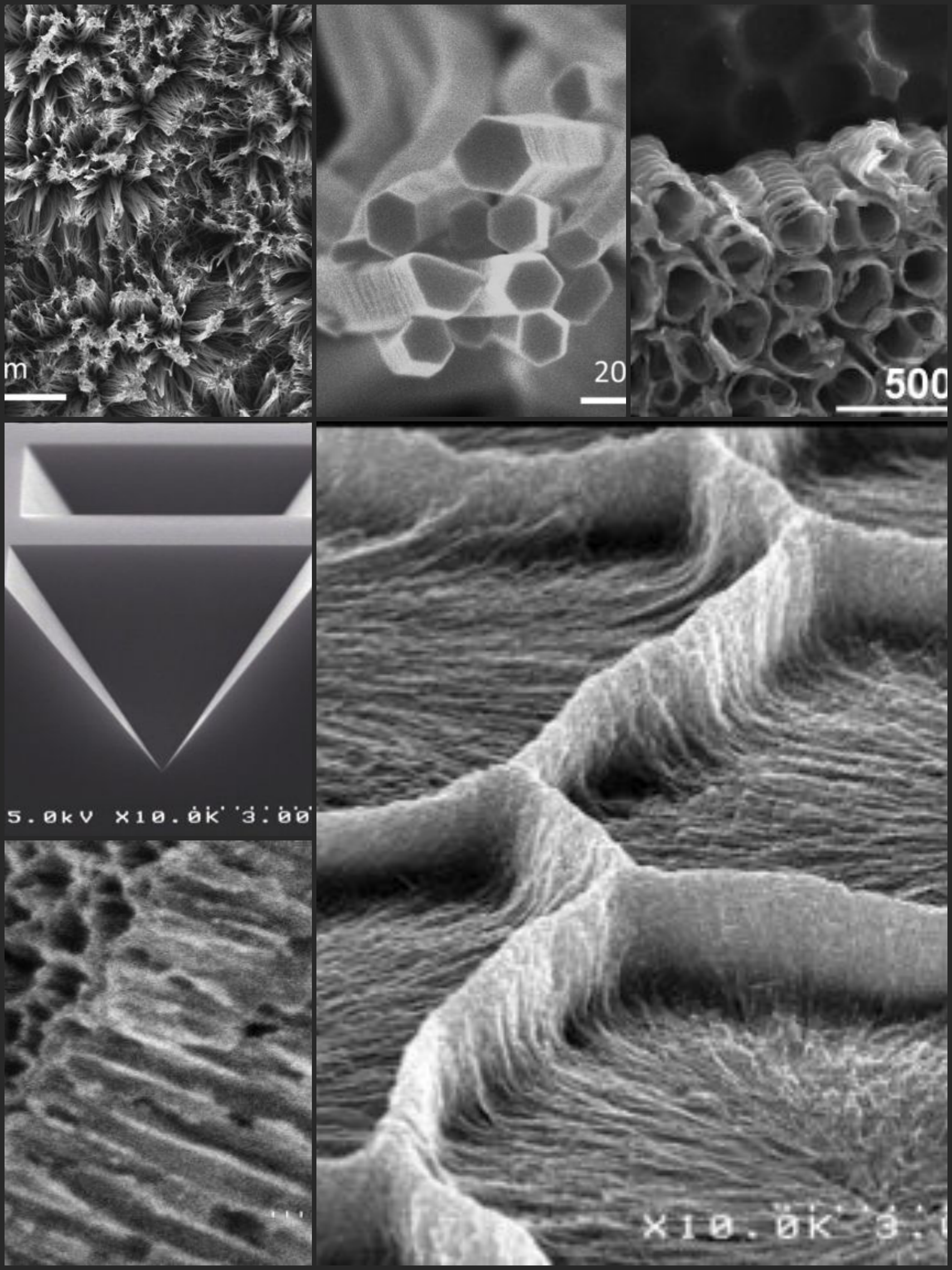
The aim of these days is to bring together at national level the French and French-speaking players involved in research into silicon and porous semiconductors/oxides and their applications.

This 5th edition of the SCOPe days will be an opportunity for our community to share our latest advances in the field and to promote the younger generation.

Les doctorants et post-doctorants seront prioritaires pour les présentations orales.

Thèmatiques abordées :
  • Elaboration, techniques de fabrication, structures
  • Luminescence et photonique
  • Microélectronique
  • Systèmes et intégration
  • Coatings fonctionnels
  • Capteurs
  • Photovoltaic
  • Matériaux d’électrodes, énergie, conversion, stockage
  • Imagerie médicale, thérapie
PRESENTATION

Un intérêt nouveau pour les semi-conducteurs poreux a émergé dans la communauté scientifique dans les années 90, notamment grâce à la découverte de la photoluminescence du Si poreux. Les procédés électrochimiques sont devenus des méthodes phares de nano-structuration de la plupart des semi-conducteurs (Si, GaAs, InP, etc…) et ont permis la génération de réseaux poreux auto-ordonnés (Al2O3, TiO2etc.). Since then, they have been widely studied because they have opened up prospects for the manufacture of nano-objects with new properties, particularly electronic and optical. Subsequently, the potential applications of these porous anode structures have continued to grow and evolve. In particular, porous Si with varied functionalities has revealed considerable potential for applications in opto- and microelectronics, systems, sensors, energy materials and nanomedicine.

Aujourd’hui, le silicium et les semi-conducteurs poreux sont au cœur des intérêts scientifiques de nombreuses équipes de recherche dans le monde entier, attirant l’attention de chimistes, de physiciens, de biologistes et de médecins.

COMITE SCIENTIFIQUE

  • BASTIDE Stéphane – ICMPE-CMTR – Université Paris-Est
  • BILLOUÉ Jérôme – GREMAN – Université de Tours
  • COFFINIER Yannick – IEMN – Université de Lille 1
  • CUNIN Frédérique – Institut Charles Gerhardt Montpellier – Université de Montpellier
  • DJENIZIAN Thierry – MADIREL – Aix Marseille Université
  • GAUTIER Gaël – GREMAN – Université de Tours
  • SANTINACCI Lionel – CiNaM – Aix Marseille Université
COMITE D’ORGANISATION

  • BASTIDE Stéphane – ICMPE-CMTR – Université Paris-Est
  • BILLOUÉ Jérôme – GREMAN – Université de Tours
  • CUNIN Frédérique – Institut Charles Gerhardt Montpellier – Université de Montpellier
  • GAUTIER Gaël – GREMAN – Université de Tours
INVITED CONFERENCES

Ciro Chiappini - King's College London - Nanomaterials and Biointerfaces Lab (UK)
"High aspect ratio porous silicon nanostructures for drug delivery and biosensing".

Anne-Chantal Gouget - Condensed Matter Physics Laboratory (France)
"Functionalization of oxide-free silicon surfaces

Yannick Coffinier - Institute of Electronics, Microelectronics and Nanotechnology (France)
"Fabrication of silicon nanostructures via MACE method and their applications".


Pour plus de renseignement : yannick.coffinier@univ-lille.fr  or  scope2019@sciencesconf.org

Logo
Cité Scientifique
Avenue Henri Poincaré
CS 60069
59 652 Villeneuve d'Ascq Cedex, France
Tel : 03 20 19 79 79
CNRS Logo University of Lille Logo University Polytech Logo Junia Logo Centrale Lille Logo Renatech Logo RFnet Logo
Site map
Copyright Service ECM et pôle SISR 2024
  • Scientific production
  • Legal information
  • Privacy policy
Faire défiler vers le haut
fr_FR
fr_FR
en_GB
We use cookies to ensure you have the best experience on our website. If you continue to use this site, we will assume that you are happy with it.OKNoPrivacy policy