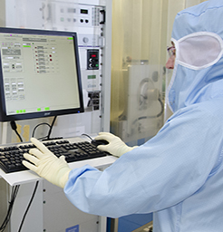
IEMN
  • Home
  • News
    • IEMN Newsletters
    • M2-Ingé Internships
    • Job offers
    • All news
  • The Institute
    • Presentation
    • Organization of the institute
    • The Scientific Department
    • The Technological Department
    • Administrative and financial management
    • Rules of procedure
    • Our commitments
  • The Research
    • Scientific departments
      • Nanostructured Materials and Components
      • Micro / nano optoelectronics
      • Telecommunications Technologies and Intelligent Systems
      • Acoustic
    • Research groups
    • Flagship
  • Scientific Production
    • IEMN publications
    • Scientific production resources
  • The platforms
    • CMNF - Central Platform for Micro Nano Manufacturing
      • Engraving and implantation pole
      • In Line Analysis Unit
      • Soft Lithography and Bio Microfluidics
      • Deposits and epitaxy division
      • Lithography Unit
      • Packaging Division
      • CMNF Staff
    • PCMP - Multi-Physics Characterization Platform
      • Scanning Probe Microscopy Facility
      • Hyperfrequency, Optical and Photonic Characterization (CHOP)
      • Advanced Communications Systems and Prototyping cluster (SigmaCOM)
      • Characterisation, ElectroMagnetic Compatibility and Prototyping Centre (C2EM)
      • PCMP Staff
    • Services offered by our platforms
  • Partnership - Valuation
    • Academic Collaborations
    • ANR Projects
    • Main international collaborations
    • Industrial partnerships
    • The joint IEMN-Industry laboratories
    • Startups
  • Research Training
    • After the thesis
      • Do a post-doc at the IEMN
      • Towards the world of business and industry
      • Become a teacher-researcher
      • Become a Researcher
      • Starting a business at IEMN
      • FOCUS on a SATT engineer from the IEMN
    • A thesis at IEMN
      • Thesis and HDR defenses
      • Thesis topics
      • Financing
      • Doctoral studies
    • Master - Engineer
      • Masters ULille
        • Master Life Sciences and Technologies graduate programme
        • Master Nanosciences and Nanotechnologies - Speciality ETECH
        • Master Networks and Telecommunications
      • UPHF-INSA Masters
        • Master in Embedded Systems and Mobile Communications Engineering
        • Master Cyber Defense and Information Security
        • Master in Materials, Control and Safety
        • Master in Image and Sound Systems Engineering
      • Partner/Tutoring Engineering Schools
      • M2-Ingé Internships
    • The Lille branch of the GIP-CNFM
    • Nano-École Lille
  • Contact Us
    • Location
    • Contact form
    • Staff directory
  • Our support
  • fr_FR
  • Rechercher
  • Menu Menu
NEWS

Research Engineer Elaboration of thin films under vacuum by PVD

Typical job
Research engineer in materials science / development
Missions The agent will be responsible for ensuring the development and proper operation of physical vapor deposition (PVD) equipment. The primary mission will be to develop materials on sputtering equipment. His secondary mission will be to work on electron gun and joule effect evaporation equipment. In collaboration with the IEMN research teams and the technical staff of the pole, he will have the task of developing, guaranteeing the durability and valorizing innovative processes in the flagship fields (sensors, IoT and microenergy, micro-nanoelectronics, MEMS/NEMS) of the laboratory. He will also ensure the safety of a specific environment (gas, RF, HT...).
Activities
  • Ensure the installation of the new sputtering equipment in collaboration with the project actors
  • Assist the existing technical staff in the management of the PVD (sputtering and evaporation) equipment in the clean room and its maintenance
  • Deposition and development of materials by PVD in collaboration with the cluster's IT and the laboratory's researchers
  • Characterize repositories with CPER actors
  • Create a process database accessible to users
  • Train the laboratory staff on the PVD equipment
  • Produce basic devices using the micro-nano-fabrication techniques available in the laboratory (lithography, deposition, etching)
  • Make presentations and reports on the progress of the work
Qualifications: To fulfill this mission, this engineer will have :

  • General knowledge of materials science
  • Specific knowledge in the elaboration of PVD thin films (reactive sputtering, evaporation by electron gun and by Joule effect)
  • General knowledge in the field of characterization (SEM, ellipsometry, profilometry, EDX, DRX, AFM, XPS)
  • Basic knowledge of micro-nanofabrication
  • Knowledge of the risks and health and safety rules relating to the equipment and materials used (gas, chemicals, RF, HT)
  • Knowledge of vacuum techniques (primary vacuum, secondary vacuum)
  • Handling of gases under pressure
  • Mastery of the English language: oral and written expression and comprehension. Minimum level B1
Context: The Institute of Electronics, Microelectronics and Nanotechnologies is a laboratory whose core activities are focused on micro and nanotechnologies and their applications in fields such as information, communication, transport, energy and health. Under the aegis of three main supervisory bodies (CNRS, University of Lille, UPHF), the IEMN is located on different sites in Villeneuve d'Ascq, Lille and Valenciennes with a staff of 450 people (170 researchers and teacher-researchers, 65 engineers and permanent technicians, 140 theses in progress).

The Micro and Nanofabrication Center (CMNF) of the IEMN is a platform of the national network of large technology centers of the CNRS, RENATECH. It is open to internal and external academic and industrial users.
The agent will be assigned to the "Deposit and Epitaxy" division of the CMNF, under the responsibility of the division manager, Mrs. Isabelle Roch-Jeune.


Host Unit:
IEMN UMR CNRS 8520
Avenue Poincaré
59652 VILLENEUVE D'ASCQ CEDEX
www.iemn.fr

Contract Type:
Technical CDD

Duration of the contract 20 months

Expected date of hire:01/11/2022

Number of hours worked :
Full-time

Compensation:
2609.40 euros gross per month
according to experience

Desired level of education:Doctorat


For further information
If you are interested in this position, please contact :

isabelle.roch-jeune@univ-lille.fr

  • Research Engineer Elaboration of thin films under vacuum by PVD
Logo
Cité Scientifique
Avenue Henri Poincaré
CS 60069
59 652 Villeneuve d'Ascq Cedex, France
CNRS Logo University of Lille Logo University Polytech Logo Junia Logo Centrale Lille Logo Renatech Logo RFnet Logo
Site map
Copyright Service ECM et pôle SISR 2024
  • Scientific production
  • Legal information
  • Privacy policy
Faire défiler vers le haut
fr_FR
fr_FR
en_GB
We use cookies to ensure you have the best experience on our website. If you continue to use this site, we will assume that you are happy with it.OKNoPrivacy policy