
III-V semiconductors (arsenides, phosphides, antimonides)
III-V semiconductors (arsenides, phosphides, antimonides)
 Materials
Wafer scale epitaxy : GaAs, AlAs, GaInAs, InAlAs, GaAlAs, InP, GaP, GaInP, InAlP, GaSb, InSb, AlSb, GaInSb, InAlSb Ternaries AsP et AsSb, GaInAsP, InAlAsSb
Selective Area Epitaxy : InAs, InSb, InP, GaInAs, GaSb, GaAsSb, GaAs
Synthesis
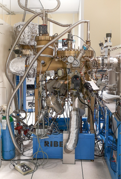
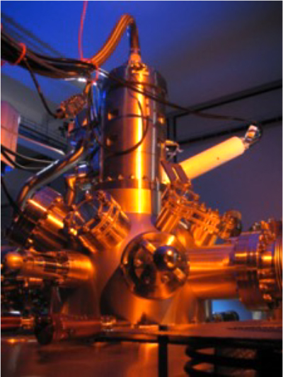
MBE C21 Riber – 3’‘ wafers – 2’‘ homogeneity – UHV – 350 to 650°C
Mastering
Complete for wafer scale epitaxy
Partial for Selective Area Epitaxy
Applications
HF electronics (HEMTs, TFETs, HBTs)
Optoelectronics (UTC PDs, thermionicdiodes)
THz (High speed photodetectors, IR modulators)
Ballistic transport, spin orbitronics, quantum simulators
Characterisation
Raman, µPL, DRX, XPS, Hall Effect, SEM, SIMS, AFM, FIB STEM
Partnership
Riber, C2N, LETI, MIT, IMEC, NEEL, CINTRA, IAF, TU Berlin, IAF, INSP, Renatech, …
Semiconducting nanocrystals and molecular networks
Semiconducting nanocrystals and molecular networks
 Materials
Silicene, Germanene, CdSe/CdS, PbSe
Synthesis
Vapor Phase Deposition under UHV from – 160 to 400°C
Chemical synthesis based on organometallics under UHV or in liquid phase from 100 to 250°C
Mastering
Exploratory
Applications
Photodetection, optical emitters, high electron mobility, (electro)luminescence
Characterisation
STM, optical spectroscopy, SEM
Partnership
Horiba, STMicroelectronics, Université de Gand
Polysilicon
Polysilicon
 Synthesis
LPCVD using SiH4– Tempress tubular furnace from 580 to 700°C – Pressure from 100 to 300mTorr
Up to 25 x 2,3 or 4 inch wafers
Mastering
Partial
Applications
Electrodes, SOI
Characterisation
Ellipsometry, SEM
Partnership
Vmicro


