
Graphene, hBN
Graphene, hBN
 Synthesis
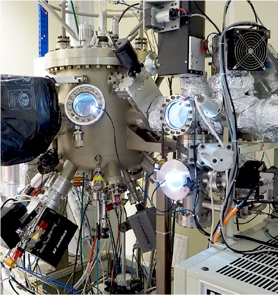
MBE C21S Riber – 3’‘ wafers – 1’‘ homogeneity – UHV – 800 to 1500°C – SiC, Ni, Ge substrates
CVD Jipélec (graphene on Cu) – 4 » wafers- 900 to 1050°C
Exfoliation for 2D heterostructures
Mastering
Complete for CVD
Partial for MBE and exfoliation
Applications
HF electronics, field effect transistors, RF switch, photodetectors
Characterisation
Raman, XPS, Hall Effect, SEM, AFM, TofSIMS
Partnership
IHP (Frankfurt/Oder), ONERA, GEMAC, SOLEIL
Transition Metal Dichalcogenides
Transition Metal Dichalcogenides
 Materials
WSe2, MoSe2, TaSe2, , ZrSe2, NbSe2, HfSe2
Synthesis
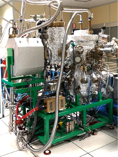
MBE 2D Vinci – UHV – 3’‘ wafers – UHV – 200 to 750°C
Exfoliation for 2D heterostructures
Mastering
Exploratory
Applications
Tunnel diodes, field effect transistors
Characterisation
Raman, µPL, DRX, XPS, UPS, SEM, AFM
Partnership
Riber, Vinci, CINTRA, C2N, CP2M


