https://www.iemn.fr/wp-content/uploads/2026/01/vignette_voeux_2026.jpg
277
388
editrice
https://www.iemn.fr/wp-content/uploads/logos/logo_IEMN.png
editrice2026-01-08 11:59:442026-01-09 09:39:31La Direction de l’IEMN vous souhaite une excellente année 2026 !
https://www.iemn.fr/wp-content/uploads/2025/05/seminar2.jpg
277
388
editrice
https://www.iemn.fr/wp-content/uploads/logos/logo_IEMN.png
editrice2025-06-10 09:19:232025-06-10 09:21:42Florian Jaroschik: ‘Modulating reactivity, luminescence and magnetic properties of organolanthanide complexes’ – 10 juin 2025
https://www.iemn.fr/wp-content/uploads/2024/10/THESES.jpg
277
547
editrice
https://www.iemn.fr/wp-content/uploads/logos/logo_IEMN.png
editrice2025-06-10 08:07:542025-06-10 09:20:56Cédric Teyssédou : Fabrication de micro-condensateurs hybrides 3D à charge rapide pour l’autonomie énergétique de composants électroniques miniaturisés – 11 juin 2025
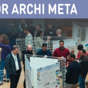
https://www.iemn.fr/wp-content/uploads/2025/02/0_base_images_mises_en_avant.jpg
277
388
editrice
https://www.iemn.fr/wp-content/uploads/logos/logo_IEMN.png
editrice2025-02-26 10:36:472025-03-04 08:54:05GDR ARCHI META du 24 au 28 février 2025
https://www.iemn.fr/wp-content/uploads/2024/01/anneephysiquefin.jpg
166
233
editrice
https://www.iemn.fr/wp-content/uploads/logos/logo_IEMN.png
editrice2024-01-26 12:25:592024-01-31 11:42:29Année de la Physique : des enseignants de Physique-Chimie en visite à l’IEMN.
https://www.iemn.fr/wp-content/uploads/2023/05/rafald_vignette-1.jpg
146
200
editrice
https://www.iemn.fr/wp-content/uploads/logos/logo_IEMN.png
editrice2023-11-02 14:28:322023-11-07 16:29:12Le 9ème Workshop RAFALD 2023 se déroulera à l’IEMN du 22 au 24 novembre 2023
https://www.iemn.fr/wp-content/uploads/2023/10/journee_puissance.png
166
250
editrice
https://www.iemn.fr/wp-content/uploads/logos/logo_IEMN.png
editrice2023-10-30 15:23:402023-11-30 12:36:521ère édition de la Journée Électronique de Puissance organisée à l’IEMN le 8 novembre de 8h30à 18h00
https://www.iemn.fr/wp-content/uploads/2023/10/vignette_montage_fete_science.jpg
158
222
editrice
https://www.iemn.fr/wp-content/uploads/logos/logo_IEMN.png
editrice2023-10-19 15:24:202023-10-20 11:46:16L’IEMN présent à la Fête de la Science
https://www.iemn.fr/wp-content/uploads/2023/10/gdr_neno-1.png
166
233
editrice
https://www.iemn.fr/wp-content/uploads/logos/logo_IEMN.png
editrice2023-10-18 13:32:032023-11-10 15:28:20Les journées Plénières du GDR NEMO à l’IEMN
https://www.iemn.fr/wp-content/uploads/2023/10/cristal_vignette.jpg
166
233
editrice
https://www.iemn.fr/wp-content/uploads/logos/logo_IEMN.png
editrice2023-10-04 10:13:112023-10-24 09:03:51Des personnels de l’IEMN lauréats de la Médaille de Cristal collectif du CNRS 2023