

Dr.-Ing. Christoph BAER & Ing. Birk HATTENHORST
Institute of Electronic Circuits
Ruhr-Universität Bochum, Universitätsstr. 150, ID 03/324
44780 Bochum – GERMANYLundi 23 April 2018 à 14h00
IEMN Salle du conseil – Villeneuve d’Ascq
Abstract :
RF-sensors and Radar systems found their way into civil and industrial applications decades ago. Since then, they reliably measure distances, velocities, and filling levels etc. contact free and with great accuracy. Lately, current trends and technological achievements pushed operating frequencies up to the millimeter wave range, which allows for the determination of various additional physical quantities. Consequently, these novel sensors can be utilized in numerous areas of process industry, civil protection, and daily life. Therefore, their main purpose will be the determination and investigation of environmental parameters that allow for the supervision of crucial system parameters and the interpretation of complex processes. The talk will give an overview on diverse RF‐sensors for different applications, which were explored at the Ruhr‐University Bochum within recent years. The presented sensor applications include: humanitarian demining, mmWave imaging, contact‐free gas sensing, as well as dust and particle determination for process industry and natural hazard protection. Next to the introduction of the numerous areas of application, the different sensor designs will be explained and their field applicability verified. Moreover, opportunities regarding student exchanges between Ruhr-University and Lille University will be introduced and discussed.
About the lecturers:
 Christoph Baer received his diploma and doctor degree in electrical engineering at Ruhr-University Bochum in 2009 and 2015, respectively. From 2006 to 2015 he worked as a research engineer on radar systems and radar applications with the Krohne Group in Duisburg, Germany. Currently, Dr. Baer is postdoctoral researcher and academic counselor with the Institute of Electronic Circuits at Ruhr-University Bochum. He is author or co-author of more than 60 international publications and holds 8 international patents. His research interests include ground penetrating radar systems and concepts, methods for humanitarian demining, RF-material characterization and synthesis, sensors for avalanche science, and industrial microwave sensors. Dr. Baer is chairman of the IEEE SIGHT Germany Section.
 Birk Hattenhorst was born in Lübbecke, Germany, in 1989. He received the M.Sc. degree in electrical engineering from the Ruhr-University Bochum, Bochum, Germany, in 2014. He has been a Research Assistant with the Institute of Electronic Circuits, Ruhr-University Bochum, since 2014. His current research interests include microwave measurement techniques, radar technology, antenna design, meta-materials and material characterization.

Dr Mickaël Tessier
Ghent university, BelgiumMercredi 17 avril 2018 à 14h00
IEMN Salle du conseil – Villeneuve d’Ascq
Abstract :
Innovative Colloidal Nanostructures: Nanoplatelets and III-V Quantum Dots
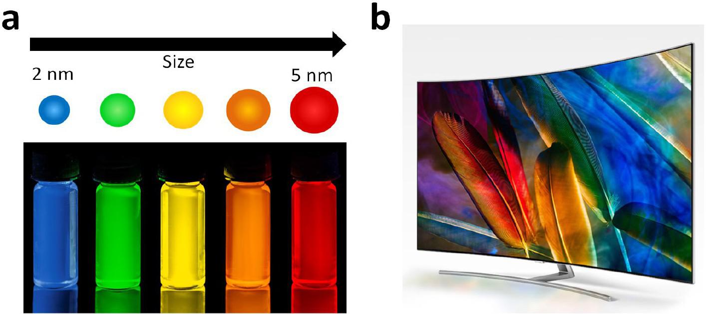
Colloidal Quantum Dots (QDs) are semiconductor nanocrystals in the 1 to 10 nm size range synthesized by wet chemistry process. Because of these small sizes, QDs are subject to quantum-size effect. This effect leads to discrete transitions, much like in an atom or a molecule, with energies higher than the bulk and that are strongly dependent of the QDs sizes. This property has allowed QDs to emerge as a novel class of optoelectronic materials over the last 25 years. The most advanced application of colloidal QDs, at least from a research valorization perspective, is their commercial use in liquid crystal displays (LCDs). First launched in 2013, sales of QDs-enhanced LCDs are expected to achieve 18 million units in 2018.
a. Vials containing QDs of different sizes under UV light. The emitted color depends of the QDs sizes. b. Commercial QDs display (http://www.samsung.com/global/tv/).
Significant advances have been made in the synthesis of QDs since the beginning of the 1990s. The shape of the nanoparticles can now be finely controlled, and nanoparticles with various shapes have been synthesized. In particular, colloidal nanoplatelets are atomically flat nanostructures that present only one dimension of quantum confinement.1In this lecture, I first present how the nanoplateletssizeand composition can be perfectly controlled via inventive synthesis protocols and how theseparameters affects the nanoplatelets optical properties.(2–4)
To facilitate the use of nanocrystals in the industry, interest is shifting from the well-characterized cadmium-based QDs to cadmium-free alternatives such as indium phosphide. We recently proposed protocols based onaminophosphine-type precursors that allow for a cost efficient, up-scaled syntheses of indium phosphide(InP) QDs of different sizes.(5) A detailed understanding of the reaction chemistry is a key in the development of colloidal QDs synthesis. I present an investigation of chemical reactions leading to the formation of InP starting from aminophosphine-type precursors.(6) This mechanism is innovative in the sense that it points out a double role of the phosphorus precursor in the reaction as both a reducing agent and the source of the phosphorus needed to form InP. Its understanding furthers the general use of aminopnictogens for the
synthesis of III-V QDs.(7) Finally, I show that InP QDs can be processed in polymer layer and that their structure can be optimized in order to obtain more efficient and cheaper lighting devices.(8)
References
(1) Ithurria, S.; Tessier, M. D.; Mahler, B.; Lobo, R. P. S. M.; Dubertret, B.; Efros, A. L. Nat. Mater.2011, 10, 936–941.
(2) Tessier, M. D.; Mahler, B.; Nadal, B.; Heuclin, H.; Pedetti, S.; Dubertret, B. Nano Lett.2013, 13, 3321–3328.
(3) Tessier, M. D.; Spinicelli, P.; Dupont, D.; Patriarche, G.; Ithurria, S.; Dubertret, B. Nano Lett.2014, 14, 207–213.
(4) Tessier, M. D.; Javaux, C.; Maksimovic, I.; Loriette, V.; Dubertret, B. ACS Nano2012, 6, 6751–6758.
(5) Tessier, M. D.; Dupont, D.; De Nolf, K.; De Roo, J.; Hens, Z. Chem. Mater.2015, 27, 4893–4898.
(6) Tessier, M. D.; De Nolf, K.; Dupont, D.; Sinnaeve, D.; De Roo, J.; Hens, Z. J. Am. Chem. Soc.2016, 138, 5923–5929.
(7) Grigel, V.; Dupont, D.; De Nolf, K.; Hens, Z.; Tessier, M. D. J. Am. Chem. Soc.2016, 138, 13485–13488.
(8) Dupont, D.; Tessier, M. D.; Smet, P. F.; Hens, Z. Adv. Mater.2017, 29, 1700686.
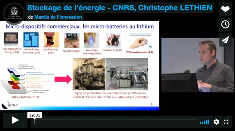
pour l’avenir de l’internet des objets, des énergies alternatives et de la mobilité.
Christophe LETHIEN, Institut d’Electronique, de Microélectronique et de Nanotechnologie, Université de Lille, CNRS.
Les Mardis de l’innovation. 20 Mars 2018.
> Visionnez la conférence sur vimeo

![]() Véritable encyclopédie vivante de l’innovation à travers le monde, destinée aux acteurs de l’innovation. Les Mardis de l’Innovation sont des cours/conférences en format ouvert portant sur la culture de l’innovation et sa mise en œuvre entrepreneuriale. Depuis dix ans, 270 cours/conférences, plus de 600 professionnels formés, plus de 10 000 auditeurs libres, 200 témoignages d’entreprises parmi les plus innovantes au monde.
Véritable encyclopédie vivante de l’innovation à travers le monde, destinée aux acteurs de l’innovation. Les Mardis de l’Innovation sont des cours/conférences en format ouvert portant sur la culture de l’innovation et sa mise en œuvre entrepreneuriale. Depuis dix ans, 270 cours/conférences, plus de 600 professionnels formés, plus de 10 000 auditeurs libres, 200 témoignages d’entreprises parmi les plus innovantes au monde.

 Rewarding excellence, innovation and success
La compagnie ALLOS semiconductors s’est vu décerner un CS Award portant sur des travaux effectués en étroite collaboration avec l’équipe de recherche du Dr Farid Medjdoub de l‘Institut d’électronique, de microélectronique et de nanotechnologie. Les derniers résultats de l’IEMN démontrent notamment une tension de claquage de plus de 1400 V pour les mesures verticales et latérales sur le prochain produit d’ALLOS, l’épiwafer GaN-on-Si pour les appareils de 1200 V.

 HABILITATION A DIRIGER DES RECHERCHES – UNIVERSITE DE LILLE
DAVY GAILLOT
27 mars à 10h30
Amphithéâtre 1A12 – IUT-A
![]() Ecole doctorale : Sciences Pour l’Ingénieur (SPI)
Ecole doctorale : Sciences Pour l’Ingénieur (SPI)
Laboratoire/Etablissement : IEMN-IRCICA, Université de Lille – FST
Discipline : SCIENCES PHYSIQUES
LES MEMBRES DU JURY :
Garant de l’habilitation :
Rapporteurs :
Examinateurs :

Par Laurent Limot
chercheur CNRS à l’IPCMS à Strasbourg
Contact : limot@ipcms.unistra.frMercredi 16 avril 2018 à 10h30
IEMN Salle du conseil – Villeneuve d’Ascq
Abstract :
Recent advances in addressing and controlling the spin states of a surface-supported object (atom or molecule) have further accredited the prospect of quantum computing and of an ultimate data-storage capacity [1]. Information encoding requires that the object must possess stable magnetic states, in particular magnetic anisotropy to yield distinct spin-dependent states in the absence of a magnetic field together with long magnetic relaxation times. Scanning probe techniques have shown that inelastic electron tunneling spectroscopy (IETS) within the junction of a scanning tunneling microscope (STM) is a good starting point to study the stability of these spin states [2]. STM-IETS allows for an all-electrical characterization of these states by promoting and detecting spin-flip excitations within the object of interest. As spin excitations need however to be preserved from scattering events with itinerant electrons, single objects are usually placed on non-metallic surfaces such as thin-insulating layers or superconductors. In this sense, new approaches to improve the detection of spin-flip excitations are desirable. With this purpose we present here a novel strategy based on the molecular functionalization of a STM tip. We study the surface magnetism of a simple doubledecker molecule, nickelocene [Ni(C5H5)2], which is adsorbed directly on a copper surface. By means of X-ray magnetic circular dichroism and density functional theory calculations, we show that nickelocene on the surface is magnetic (Spin = 1) and possesses a uniaxial magnetic anisotropy, while IETS reveals an exceptionally efficient spin-flip excitation occurring in the molecule [3]. Interestingly, nickelocene preserves its magnetic moment and magnetic anisotropy not only on the surface, but also in different metallic environments. Taking advantage of this robustness, we are able to functionalize the STM tip with a nickelocene [3,4], which can then be employed as a portable source of inelastic excitations. As we will show during the talk, IETS can then be used to probe the interaction between a surface-supported object and the nickelocene tip, including a magnetic interaction.
M. Ormaza1, P. Abufager2, B. Verlhac1, N. Bachellier1, M.-L. Bocquet3, N. Lorente4, and Laurent Limot1,*
1Université de Strasbourg, CNRS, IPCMS, UMR 7504, F-67000 Strasbourg, France
2Instituto de Física de Rosario, CONICET, Universidad Nacional de Rosario, Argentina
3Ecole Normale Supérieure, UPMC Univ. Paris 06, CNRS, 75005 Paris, France
4CFM/MPC and DIPC, 20018 Donostia-San Sebastián, Spain
References
[1] F.D. Natterer et al., Nature 543, 226 (2017); T. Choi et al., Nat. Nanotech. 6 (2017)
[2] A.J. Heinrich, J.A. Gupta, C.P. Lutz, and D.M. Eigler, Science 306, 466 (2004)
[3] M. Ormaza et al., Nano Lett. 17, 1877 (2017)
[4] M. Ormaza et al., Nat. Commun. 8, 1974 (2017)

Dr. HO-JIN SONG, Pohang University of Science and Technology (POSTECH)
Tuesday 5 April at 10h30
Conférence 10:30
Anfiteather – IEMN-LCI Institut d’Electronique, de Microélectronique et de Nanotechnologie U.M.R C.N.R.S 8520 – Laboratoire Central – Cité Scientifique – Avenue Poincaré – CS 60069 – 59652 VILLENEUVE D’ASCQ CEDEXIntervenants
- Dr. HO-JIN SONG, Pohang University of Science and Technology (POSTECH), Korea