A magnetoelectric random access memory cell based on the stress-mediated magnetoelectric effect that promises extremely low bit-reading and low bit-writing energies.
WASHINGTON, D.C., May 30, 2017 — Today’s computers provide storage of tremendous quantities of information with extremely large data densities, but writing and retrieving this information expends a lot of energy. More than 99 percent of the consumed power of information storage and processing is wasted in the form of heat, a big headache that still has not abated.
A team of researchers from France and Russia has now developed a magnetoelectric random access memory (MELRAM) cell that has the potential to increase power efficiency, and thereby decrease heat waste, by orders of magnitude for read operations at room temperature. The research could aid production of devices such as instant-on laptops, close-to-zero-consumption flash drives, and data storage centers that require much less air conditioning. The research team reported their findings this week in Applied Physics Letters, by AIP Publishing.
Billions of transistors can now be etched onto single chips in a space the size of a dime, but at some point, increasing this number for even better performance using the same space will not be possible. The sheer density of these nanoscopic transistors translates into more unwanted heat along with quantum-level interactions that must now be addressed.
Over the last several years, research has ramped up to explore the magnetic properties of electrons in a phenomenon called the magnetoelectric effect. This effect, often of interest in the field of research known as spintronics, takes advantage of an electron’s spin, instead of its charge. Spins can potentially be manipulated at smaller size scales using far less energy.
Most efforts have focused on reducing the energy of the write operations in magnetic memories, since these operations typically use more energy than read operations. In 2010, the same French and Russian team showed that a combination of magnetoelastic and piezoelectric materials in a magnetoelectric memory cell could allow a 100-fold reduction of the energy needed for the writing process. In the researchers’ latest paper, they show that the same magnetoelectric principle also can be used for read operations with extra-low energy consumption.
“We focused on read operations in this paper because the potential for the writing energy to be very low in magnetoelectric systems means that the energy output will now be higher for read operations,” said Nicolas Tiercelin, co-author of the paper and a research scientist from the Centre national de la recherche scientifique (CNRS) who is conducting research at the Institute of Electronics, Microelectronics and Nanotechnology in Lille, France.
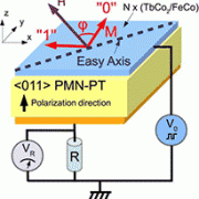
The core of the researchers’ MELRAM memory cell is based on combining the properties of two types of materials by coupling them mechanically. Magnetic alloys — one based on a combination of terbium-cobalt and the other based on iron and cobalt — with thicknesses of a few nanometers are stacked on top of one another. The alloys form a magnetoelastic nanocomposite material whose magnetic spins react to mechanical stress.
These alloys are then placed on a piezoelectric substrate, which consists of relaxor ferroelectrics, exotic materials that change their shape or dimensions when they are exposed to an electric field.
“Together, these materials constitute multiferroic heterostructures in which the control of the magnetic properties is made possible by the application of an electric voltage,” Tiercelin said.
“The nanocomposite multilayer provides strong magnetoelectric interaction at room temperature,” said Vladimir Preobrazhensky, another co-author of the paper and research director at the Wave Research Center, Prokhorov General Physics Institute of the Russian Academy of Sciences in Moscow. “This interaction is the basic mechanism for control of magnetic states by the electric field. This feature of the magnetoelectric memory is the origin of its extra-low power consumption.”
This research was carried out within the scope of the International Associated Laboratory on Critical & Supercritical phenomena in Functional Electronics, Acoustics & Fluidics – LIA LICS.
_______________________________________________________________
Alexey Klimov,1,2,3 – Nicolas Tiercelin,2 – Yannick Dusch,2 – Stefano Giordano,2 – Theo Mathurin,2 – Philippe Pernod,2 – Vladimir Preobrazhensky,2,4 – Anton Churbanov,1,5 – Sergei Nikitov,1,5
ABSTRACT
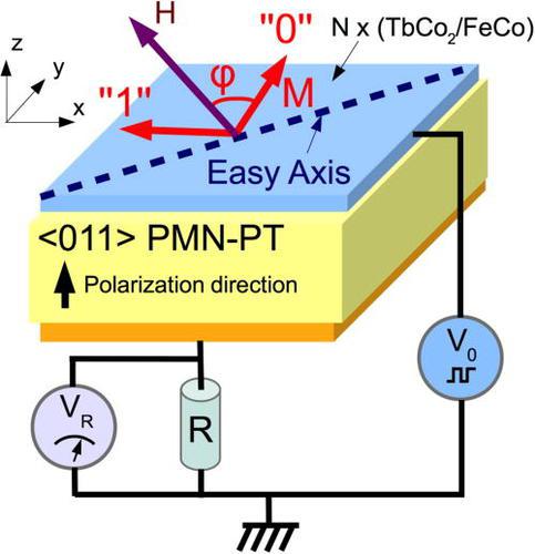
MELRAM cell and the electric scheme for the magnetic state identification
Magnetic memory cells associated with the stress-mediated magnetoelectric effect promise extremely low bit-writing energies. Most investigations have focused on the process of writing information in memory cells, and very few on readout schemes. The usual assumption is that the readout will be achieved using magnetoresistive structures such as Giant Magneto-Resistive stacks or Magnetic Tunnel Junctions. Since the writing energy is very low in the magnetoelectric systems, the readout energy using magnetoresistive approaches becomes non negligible. Incidentally, the magneto-electric interaction itself contains the potentiality of the readout of the information encoded in the magnetic subsystem. In this letter, the principle of magnetoelectric readout of the information by an electric field in a composite multiferroic heterostructure is considered theoretically and demonstrated experimentally using [N×(TbCo2/FeCo)]/[Pb(Mg1/3Nb2/3)O3](1−x)−[PbTiO3]x stress-mediated ME heterostructures.