Fast X-ray nanotomography with sub-10 nm resolution, a powerful imaging tool for nanotechnology and electrochemical energy storage
Tomographic analysis of a 3D electrode.
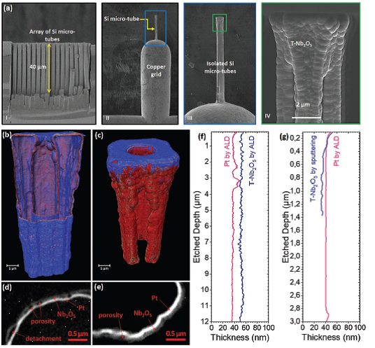
a) Preparation and analysis by double beam microscopy of a 3D Si / Al2O3 / Pt / T-Nb2O5 electrode.
b,c) 3D reconstruction by TXM of a T-Nb2O5 electrode deposited by ALD (b) and by DC magnetron sputtering (c) on a silicon micro-tube array covered with an Al2O3 / Pt stack deposited by ALD. Pt and T-Nb2O5 are shown in blue and red, respectively.
d,e) Zooms on cross sections of the samples prepared by ALD (d) and magnetron sputtering (e).
f,g) Profiles of the average thickness of Pt and T-Nb2O5 as a function of micro-tube depth.
Abstract:
During the last decade, transmission x-ray microscopes have been put into operation in most of the world’s synchrotrons. They are exceptional tools for non-invasive three-dimensional characterization of materials. However, their spatial resolution has not improved for many years, while new functional materials and micro-devices show ever finer nanostructures. In a recent work, fast (85 min) 3D tomographic acquisitions were performed with a spatial resolution of less than 10 nm. This technique, which reduces the gap between X-ray microscopy and electron microscopy, has been used to study the morphology and conformality of thin films deposited by ALD (Atomic Layer Deposition) or magnetron sputtering on silicon micro-tubes, for electrochemical energy storage applications.
Article
The potential of Transmission X-Ray Microscopes (TXM) in nanometer resolution ranges has been demonstrated by a team from IEMN, CIRIMAT and APS synchrotron in Chicago for electrochemical energy storage micro-devices based on 3D niobium pentoxide (T-Nb2O5) electrodes.
This study investigated the suitability of two different deposition methods compatible with the microelectronics industry for large-scale component production (ALD atomic layer deposition and magnetron sputtering). A single micro-tube coated with Al2O3, Pt and T-Nb2O5was plated on a copper substrate using a FIB (Focussed Ion Beam) preparation performed at IEMN..
The tomographic analysis by TXM with nanometric resolution was performed on the Argonne synchrotron (Advanced Photon Source) in Chicago and confirmed the importance of using conformal deposition methods to cover substrates or surfaces with complex geometries. As such, the evolution of the thickness of the T-Nb2O5 electrode deposited by ALD or magnetron sputtering was measured as a function of the depth of a silicon micro-tube. The TXM analysis confirms that sputtering cannot be used to conformally coat high aspect ratio 3D silicon skeletons.
Vincent De Andrade, Viktor Nikitin, Michael Wojcik, Alex Deriy, Sunil Bean, Deming Shu, Tim Mooney, Kevin Peterson, Prabhat Kc, Kenan Li, Sajid Ali, Kamel Fezzaa, Doga Gursoy, Cassandra Arico, Saliha Ouendi, David Troadec, Patrice Simon, Francesco De Carlo, and Christophe Lethien
- Fast X-ray Nanotomography with Sub-10 nm Resolution as a Powerful Imaging Tool for Nanotechnology and Energy Storage Applications
- Advanced Materials 33, no. 21, 2008653 (2021).
- https://dx.doi.org/10.1002/adma.202008653


