ScAlN as an Emerging Material System for High-Performance GaN-Based Electronics
Recent research at IEMN and its partner institutions underscores the emergence of scandium aluminium nitride (ScAlN) as a disruptive material system for next-generation III-nitride electron devices, especially high-electron-mobility transistors (HEMTs).
While ScAlN has already gained industrial traction in acoustic-wave filters, its wide bandgap, strong polarization, and potential ferroelectricity are now driving a shift toward its use in high-frequency and high-power GaN-based heterostructures. The innovation lies in leveraging these intrinsic material advantages—combined with advances in epitaxial growth—to surpass the performance limitations of established AlGaN- and InAlN-based HEMT technologies.
The principal motivation for integrating ScAlN into GaN heterostructures is its ability to induce exceptionally high two-dimensional electron gas (2DEG) densities. When grown lattice-matched to GaN at high aluminium content, ScAlN enables carrier concentrations up to twice the value achievable with InAlN. This amplitude of polarization-driven charge density is critical for short-channel scaling, mitigating short-channel effects and enabling transistor operation deep into the millimeter-wave regime.
A key technological innovation is the use of ammonia-source molecular beam epitaxy (MBE) to grow ScAlN/GaN heterostructures with high crystal quality, precise stoichiometry control, and low contamination levels. Our partner CRHEA demonstrated that Sc incorporation remains stable across a broad 180°C temperature window, and that the resulting layers exhibit low strain and high crystalline integrity. These results highlight ammonia MBE as a strategically important alternative to plasma-assisted MBE and MOCVD, the latter limited by the absence of suitable scandium precursors.
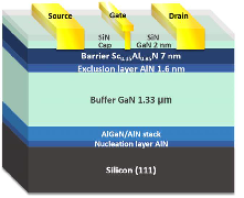
Building on this growth capability, IEMN team reports the fabrication of the first high-frequency ScAlN/GaN HEMTs produced by ammonia MBE. Initial devices exhibit 2DEG densities of 3–4 × 10¹³ cm⁻² using ~10 nm ScAlN barriers, with electron mobilities between 500 and 1000 cm² V⁻¹ s⁻¹. The introduction of ultrathin AlN or GaN capping layers represents another significant innovation, mitigating the inherent oxidation susceptibility of ScAlN without compromising electron transport. These capped heterostructures enable stable processing, leading to short-gate HEMTs (75 nm) on silicon with a maximum oscillation frequency exceeding 100 GHz, drain current density of 1.35 A mm⁻¹, and transconductance of 284 mS mm⁻¹—performance metrics that position ScAlN/GaN HEMTs as strong candidates for Ka-band applications. Power performance are evaluated at 10GHz for the first time on this material system : a saturated power of 1W.mm-1 is obtained, and further improvement is foreseen since material/technological locks are identified.
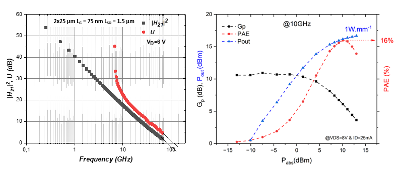
Frequency (Sij) and power performance of 75nm-gate ScAlN/GaN HEMT
Looking ahead, the research program anticipates broader integration of ScAlN into power-switching devices. Further innovation is expected through co-integration of piezoelectric, ferroelectric, and electronic functionalities enabled by ScAlN and quaternary ScAlGaN alloys. Collectively, the work delineates a rapidly expanding frontier in III-nitride materials research, driven by the unique electronic, structural, and multifunctional attributes of ScAlN and by development of dedicated technologies for its integration in future RF chips.

[1] El Whibi, S., « ScAlN/GaN-on-Si (111) HEMTs for RF applications », Applied Physics Express, vol. 18, n° 4, art. n° 046501, IOP, 2025.


