Suspended membranes machined by laser ablation to boost the performance
of radio frequency circuits
Driven since the 70’s by the monolithic miniaturization of transistors (More-Moore era), then consolidated by the second wind of microsystems in the mid-90’s (More-than-Moore era), the electronics industry is now facing a new challenge, that of autonomous, functional and miniaturized systems, giving birth to the ‘System Moore’ paradigm.
In this context, laser machining completes the portfolio of microstructuring processes by occupying the dimensional gap between the micron and the millimeter that microelectronic processes leave vacant. This experimental study shows how laser ablation allows the suspension of radio frequency chips in ultra-thin membranes, giving them exceptional electrical performance gains.
Arun Bhaskar, Justine Philippe, Flavie Braud, Etienne Okada, Vanessa Avramovic, Jean-Francois Robillard, Cedric Durand, Daniel Gloria, Christophe Gaquiere, and Emmanuel Dubois, Large-area femtosecond laser milling of silicon employing trench analysis, OPTICSAND LASER TECHNOLOGY 138 (2021).
Laser machining closes the µm-mm gap
Ultra-compact systems, such as smartphones or smartwatches, integrate a host of components and sensors covering dozens of communication, signal processing and detection functions. These components are, in most cases, from dissimilar technologies requiring heterogeneous assembly. The term ‘System Moore’ refers to this new paradigm of ultra compact integration of electronic systems. It places packaging at the center of the issues, no longer as a simple encapsulation function, but as a functional component. It implements dimensions ranging from the micron to the millimeter where a technological and economic gap exists. On the one hand, planar microelectronics technologies are expensive, oversized and unable to handle the thickness of materials. On the other hand, conventional methods of forming and machining materials reach their limits below the millimeter. In this context, laser micromachining completes the portfolio of microstructuring processes for microelectronics by occupying the ‘µm-mm’ gap. This experimental study shows how laser ablation enables backside machining of radio frequency chips whose ultimate thickness membrane suspension reduces losses and nonlinear effects associated with the silicon carrier substrate. Implemented after the full completion of the monolithic CMOS circuit manufacturing flow, this laser process enters fully into a functional packaging logic.
Suspended membranes boost RF performance
The literature reports new use cases of femtosecond silicon micromachining techniques for various applications such as microfluidics, photovoltaics, integrated circuit characterization, hydrophobic surface conditioning and laser cutting of microelectronic chips without wasting active surface. In this case, the application concerned the fabrication of suspended membranes of SOI-CMOS RF circuits/functions on SOI (Silicon-on-Insulator) substrates. From an electrical point of view, despite the presence of an insulating layer (BOX), the carrier substrate degrades the electrical performance because it offers a parasitic coupling path to the RF signals. By locally removing the carrier substrate under the active area of the sensitive circuits, they can be suspended in the form of a membrane.
At this point, the thickness of the active layer is ultimate, keeping only what is necessary to preserve the initial electronic function, namely, the active layers of the transistor and its interconnection network. The motivation for such a membrane process has been to obtain greatly improved RF performance by reducing dissipative losses, reducing substrate-induced nonlinearities and reducing parasitic capacitive coupling within the device or between devices (crosstalk). These three improvement factors have a major impact on the front-end of mobile communication systems for which more and more demanding specifications are required with the extension of frequency bands up to 6 GHz and in the millimeter range (24-48 GHz).
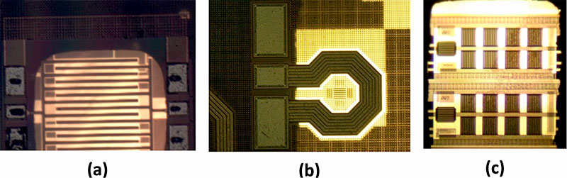
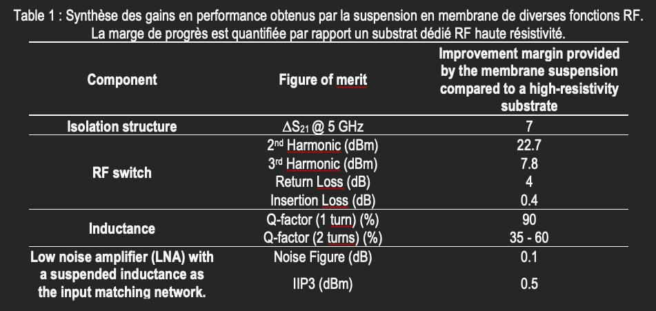
From a technological point of view, a preliminary step of optimization of the laser machining process has been implemented in order to obtain a precise control of the volume of material removed. This is the specific object of the article referenced in this commentary. The strategy consisted in systematically studying five parameters characterizing the properties of a trench structured by a laser spot scan, namely, its depth, width, roughness as well as the volume rate of material removal and the volume of redeposited residues. From a fundamental point of view, the work allowed to highlight two ablation regimes, soft and strong, depending on the fluence (energy per unit area) of the laser beam (Fig.1). The laser firing rate is another parameter whose impact is preponderant. It has been shown that for the same fluence, a high firing frequency (f=200kHz) has a negative impact on the ablation efficiency and the machining quality compared to a low frequency (f=30kHz). The explanation for this phenomenon is that the material ejecta disturb the incident beam at high frequencies (Fig.2). The suspended membranes associated with different RF circuits are presented in Fig.3. The performance gains are summarized in Table 1 with reference to a high-resistivity silicon substrate. Among the first-order results, one can note an improved rejection of ~23 and ~8 dB of the 2nd and 3rd harmonic spurious signal level. A near doubling of the quality factor (Q) is observed for the single-wound inductors. The improvement in quality factor in these proportions is of primary interest for low noise amplifiers (LNAs) whose noise figure and linearity (IIP3), two figures of merit that are particularly difficult to improve, show a 0.1 dB and 0.5 dB improvement, respectively.
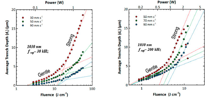
Fig.1: Average depth of trenches machined by infrared laser scanning (1030nm) as a function of fluence for different scanning speeds and two firing rates (left) frep=30 kHz and (right) frep=200 kHz. The dashed lines highlight the two ablation regimes as well as the threshold energy.
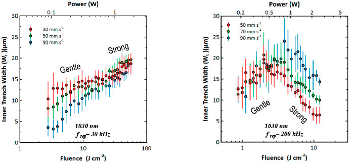
Fig. 2: Width of trenches machined by infrared (1030nm) laser scanning as a function of fluence for different scanning speeds and two firing rates (left) frep=30 kHz and (right) frep=200 kHz. A high firing rate degrades the trench aperture at high fluence due to the interaction between the material ejecta and the incident beam.


