New RF switches pave the way for 6G
The digital revolution we are experiencing is based on the transmission of an enormous amount of data, at ever increasing speeds. It is this flow of information that allows us, for example, to stay in touch with our loved ones or to work remotely during the recent health crisis. However, this connectivity has an important environmental cost because the energy consumption linked to our electronic objects is constantly increasing. Access to non-renewable raw materials at the heart of electronic chips has become a major issue in international politics.
Research laboratories of the University of Lille, and more particularly the Institute of Electronics, Microelectronics and Nanotechnology (IEMN UMR-CNRS 8520) and the Laboratory of Physics of Lasers, Atoms and Molecules (PhLAM UMR-CNRS 8523) have been developing for several years components and devices for very high speed communications
In a collaboration with the University of Texas-Austin, researchers from the University of Lille (IEMN and PHLAM) have developed and characterized a new type of switch/switch based on two-dimensional (2D) materials, for very high speed applications around 300 GHz. This device has attracted considerable attention as it has been shown to meet the requirements of future 6G communications systems. These switches are key components of reconfigurable communication systems. They are extremely common in electronic devices, performing many functions. They are, for example, the reason why smartphones switch from Bluetooth to Wi-Fi, from 3G to 4G or 5G.
Active part of the switch
The structure of the proposed switch, which is extremely simple (see illustration fig.1), uses a single layer of molybdenum disulfide (MoS2) of atomic thickness separating two metal electrodes. By optimizing the dimensions of the device, a low control voltage allows the device to be switched to a given logic state. The switch behaves like a resistive memory, which requires no holding voltage in a given logic state. Therefore the device is very energy efficient, compared to current components.
The integration of the device in a propagation line allowed us to perform electrical characterizations up to 480 GHz. The integration of the component in a data transmission system allowed us to validate the different IEEE 802.15.3d standards of the 6G standard, with a carrier at 320 GHz and data rates of 100 Gbits/s. All measurements were performed on the IEMN platform, and the device fabrication at the University of Texas-Austin.
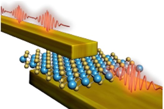
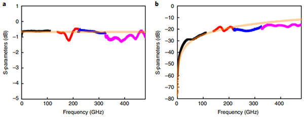
Fig.2 : Characterization of the switch in the ON state (a) and in the OFF state up to 480 GHz.
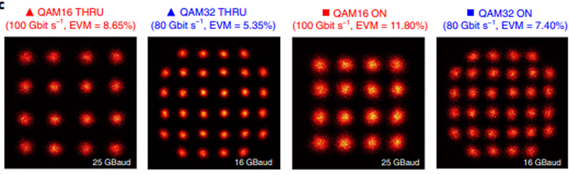
Fig.3: Illustration of the constellation diagrams obtained for a carrier at 320 GHz. The switch is in the ON state.
You will find more details in the article of the magazine NATURE Electronics in June 2022.
Kim, M., Ducournau, G., Skrzypczak, S. et al. Monolayer molybdenum disulfide switches for 6G communication systems. Nat Electron 5, 367–373 (2022).
https://doi.org/10.1038/s41928-022-00766-2
This publication is a follow-up to another recent collaborative publication
Kim, M., Pallecchi, E., Ge, R. et al. Analogue switches made from boron nitride monolayers for application in 5G and terahertz communication systems. Nat Electron 3, 479–485 (2020).
https://doi.org/10.1038/s41928-020-0416-x
Co-signatories:
IEMN : Guillaume Ducournau, Simon Skrzypczak, Henri Happy et Emiliano Pallecchi
PhLAM : Pascal Szriftgiser


