« Eternity is long, especially toward the end: another short story of Moore’s Law »
« I would have gladly attributed the first part of the title of this editorial to Michel Audiard before learning that the author of this quote is none other than the Austro-Hungarian writer Franz Kafka. You will therefore set your reading level at the height you wish, somewhere between the lightness of the former and the often sinister universe of the latter.
Alternatively, a variation of this title could have been « No exponential is forever: but forever can be delayed » whose authorship goes to Gordon Moore (Intel), eponymous author of the law discussed here. » But who enacted this law that everyone thinks they know but very few manage to state its content? Moore’s law is the story of the formidable industrial revolution that originated in the miniaturisation of integrated circuits, which today contain billions of transistors. It is also the law that governs the digitalisation of our society. Here is a short history…
The origin of Moore’s Law
It was on the basis of a small set of data, while he was an employee of Fairchild, that G. Moore had empirically formulated around 1965, that increasing the integration density by a factor of two at regular intervals would allow minimizing the manufacturing cost per unit transistor with a gain in frequency performance. Starting with a 32-component integrated circuit in 1964, Moore came back to support his projection in 1975 at the IEDM (a conference driven by a strong industrial audience): a 65,000-transistor memory circuit from Intel’s manufacturing lines confirmed his prediction of exponential growth. It was in this context that Moore’s metronome started to beat with a roadmap that made the increase of integration density and performance on the one hand, and the reduction of cost/bit on the other hand, resonate.
At the same time, R. Dennard (IBM) theorized the scaling law of the MOS transistor, which demonstrated that its power density remained constant with the reduction of its dimensions (and at the same operating frequency!). Dennard’s work confirmed the promise of a doubling of the integration density and a 40% gain in frequency for a homothetic reduction of √2% in the dimensions of the transistor and an increase in the channel doping in the same proportion.
Moore’s Law became a self-fulfilling prophecy, and the semiconductor industry devoted itself to anticipating the development of new processes and equipment, especially lithography. Never before has an industry had such a well-defined roadmap, with a trajectory that sets both the technical and economic rules of the game.
The road was full of challenges and technological obstacles: we knew where we were going without having all the keys to get there, but we were going! Aware of the challenges posed by the continuation of Moore’s Law, the world semiconductor industry agreed in 1993 to formalize the ITRS roadmap (International Technology Roadmap for Semiconductors), which allowed precise quantified objectives to be set on a quasi-irrevocable schedule. Thus the first ITRS technology node was positioned on a pattern size (the gate length in first intention) of 0.5 μm, projected 300,000 gates per chip, anticipated DRAM and SRAM memories of 16 and 4 Megabits, respectively, all for a cost of $4 per cm2! The regular interval, mentioned above, was now set at three years to progress from one technological node to the next.
The Happy Scaling Saga
For three decades, the world semiconductor industry was like a long, quiet river, with unprecedented growth made possible by the simple reduction in the geometry of the unitary MOS transistor. But everything has an end! This so-called Happy Scaling period could almost be compared to the post-war « trente glorieuses », with a thirty-year time lag. Indeed, at the beginning of the 2000s, the first pitfalls of the simple geometrical scaling law appeared with an accumulation of second-order physical effects that were now taking center stage: reduction of carrier mobility with the level of channel doping, leakage of the SiO2-based gate oxide under 3 nm thickness, parasitic depletion of the polysilicon gate.
The inventiveness of the industrial and academic microelectronics community responded to this by implementing technological boosters such as mechanical constraints, high-permittivity dielectrics and metal grids. At the same time, a second major challenge appeared: even if Dennard’s rules expressed that the energy consumed by an elementary gate is reduced by the scaling factor, the heat dissipation limited the clock frequency to around 3GHz. The solution to this challenge was to increase the number of microprocessor cores in order to favor parallel processing of binary operations.
Marked by the first hiccups in the unstoppable progress of Moore’s Law, the early 2000s were also the moment of an intense period of reflection giving rise to two complementary paradigms: Beyond CMOS and More-than-Moore. The first is fundamental in that it introduces a break with the material of choice, silicon. It includes 360-degree research on devices, materials and information processing methods (tunnel FETs, spintronics, superconductivity, molecular electronics, graphene, carbon nanotubes, chalcogenide, topological materials, photonics and optical computing, etc.). In spite of the great richness of the investigated tracks, it is not an offense to this quality research to observe that none of them has supplanted silicon technologies. The second paradigm breaks the logic of the race for size as the sole driver of growth and innovation. It consists of integrating a wide variety of functions into an autonomous system, either in a monolithic integration logic (SoC System-on-Chip, everything on the same silicon chip) or by favoring the heterogeneous integration of functions whose manufacturing constraints are incompatible (SiP System-in-Package).
Despite its first health problems, Moore’s Law continued to unfold with the introduction of new innovations aimed at strengthening the electrostatic integrity of the transistor, i.e., its ability to fully play its role as a switch without prohibitive leakage current in the blocked state. The Silicon-on-Insulator (SOI) substrate was thus to reach its age of reason after 25 years of development, with the cost/benefit balance finally tipping in the right direction. Numerous solutions for the architecture of the unitary transistor were proposed, all aiming at reinforcing the control of the field effect by a gate encasing a thin and/or narrow channel. At the beginning of the 2010 decade, the finned transistor architecture (FinFET) was the big winner of this revolution, which made the planar transistor structure on a solid substrate obsolete. Due to its conservative planar construction, the Fully-Depleted SOI (FDSOI) MOS pushed by STMicroelectronics continued to play a particularly interesting accessory role due to its back-gate control, which allows it to modulate the power/speed trade-off on demand.
Europe’s inclination for the More-than-Moore
There have been many articles predicting the end of Moore’s Law for more than 20 years for reasons that research and industry have swept aside. However, common sense leaves room for doubt when observing that the critical dimensions of MOS technologies flirt dangerously with the granularity of the material.
With a silicon mesh parameter of 0.543 nm, would this mean that the 2 nm node transistor unveiled by IBM in May 2021 has only 4 meshes? Already marked by quantization effects, would the operation of the transistor become completely quantum? How can we control, under these conditions, the variability introduced by the stochastic nature of the manufacturing steps? Would the transistor be vulnerable to a simple point defect?
Fortunately, these extremes have not been and will not be reached. The reason is that the technology node of 1993 is not compared to the technology node of 2021 in the same way. With the introduction of three-dimensional structures such as FinFET, the node qualification has shifted from a geometric definition to a scale by equivalence. Thus the 5 nm FinFET node industrialized by Intel, Samsung or TSMC displays a gate length of about 18 nm while the projections of the IRDS, which relay the ITRS since 2015, reveals a counter blocked at 12 nm for the 0.7 nm node in 2034!
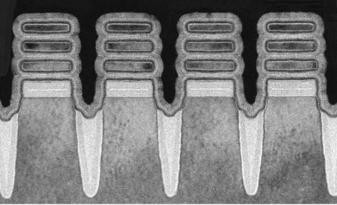
Introducing the world’s first 2 nm node chip https://research.ibm.com/blog/2-nm-chip
Anecdotally, inspection of the figures to the right and below reveal a disturbing similarity. For the 2nm node recently publicized by IBM-Research, these illustrations show that the keys to optimizing stacked nanoribbon transistors with a coated gate had been perfectly identified in the work of a thesis defended in 2009 as part of a CIFRE STMicroelectronics agreement. This raises a legitimate question: why has this type of architecture, which has been positioned as the successor to FinFET, not been pushed to the end of its development in the European ecosystem? You will not have missed the detail in the previous enumeration that the list of industrial competitors capable of sustaining the historical slope of Moore’s law is now reduced to two or three, whereas there were still ten in 2010-2012.
A major player in European microelectronics such as STMicroelectronics quickly realized that the path of diversification (More-than-Moore) would enable it to design more adapted and efficient solutions for specific needs and uses. An emblematic example is the automotive industry, where vehicles are crammed with electronic components (microcontrollers, radars, lidars, cameras, multimedia, cybersecurity, artificial intelligence, connectivity, power, etc.) ranging from 180 for the bottom of the range (Dacia) to more than 2400 for the top of the range (Mercedes). As in many applications, advanced 5nm technologies are not required to optimize specialized functions.
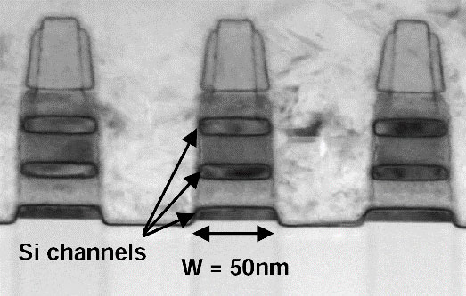
Figures taken from Emilie Bernard’s thesis defended in Jan 2009 as part of a CIFRE STMicroelectronics thesis
It is in this context of diversification that IEMN has been supporting STMicroelectronics since 2003 in a Joint Laboratory structure where four major themes are developed:
1) Potential of silicon technologies for RF and millimeter, 2) Communicating systems and embedded artificial intelligence, 3) Small-scale metrology by high-frequency acoustics, and 4) Functional and micro-thermal packaging. Our common goal is twofold: high scientific ambition and high industrial relevance. All of this with the secret hope, while remaining humble in our place, of contributing to the building of European semiconductor sovereignty, …
For more information: if you are interested in a synthesis of a remarkably clear vision of the semiconductor industry, the dossier of the Académie des technologies will provide you with many keys to understanding, in particular the European Chips Act of the European Commission. ( https://www.academie-technologies.fr/publications/les-technologies-materielles-supports-du-numerique-futur-trois-questions/ )


