New orientation for gallium nitride on silicon transistors
The first millimeter-wave power demonstration of aluminium gallium nitride/gallium nitride (AlGaN/GaN) high-electron-mobility transistors (GaN) grown on a (110) silicon substrate has been claimed by a French team of researchers [A. Soltani et al, IEEE Electron Device Letters, published online 7 March 2013]. The team consists of workers from Institut d’Electronique, de Microélectronique et de Nanotechnologie (IEMN) and Centre de Recherche sur l’Hétéro-Epitaxie et ses Applications (CRHEA).
__
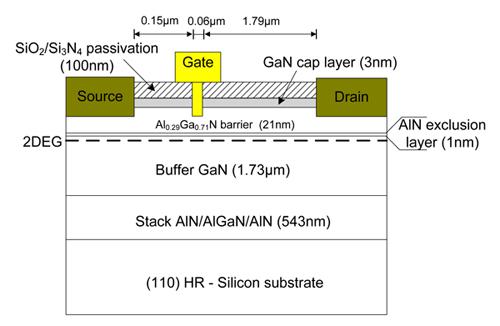
Fig.1: Structure of the AlGaN/GaN HEMT on (110) oriented silicon substrate.
__
__
Fig.2: SEM picture of the T-shaped 60 nm gate length fabricated with the nitride-gate technology
__
http://www.semiconductor-today.com/news_items/2013/MAR/IEMN_210313.html
Author(s): Soltani, A.
Institute of Electronics, Microelectronics and Nanotechnology, Centre National de Recherche Scientifique (IEMN/CNRS), Villeneuve d’Ascq, France
Gerbedoen, J.-C.; Cordier, Y.; Ducatteau, D.; Rousseau, M.; Chmielowska, M.; Ramdani, M.; De Jaeger, J.-C.


