IEMN
  • Accueil
  • Actualités
    • Newsletters de l’IEMN
    • Offres de Stages M2-Ingé
    • Les offres d’emplois
    • Toutes les actualités
  • L’Institut
    • Présentation
    • Organisation de l’institut
    • La Direction Scientifique
    • La Direction Technologique
    • La direction administrative et financière
    • Règlement intérieur
    • Nos engagements
  • La Recherche
    • Les départements scientifiques
      • Matériaux Nanostructures et Composants
      • Micro/nano et optoélectronique
      • Technologies des télécommunications et Systèmes intelligents
      • Acoustique
    • Les groupes de recherche
    • Les projets phares
  • Production Scientifique
    • Publications IEMN
    • Ressources production scientifique
  • Les plateformes
    • CMNF – Plateforme Centrale de Micro Nano Fabrication
      • Pôle Gravure et implantation
      • Pôle Analyse In Line
      • Pôle Soft Lithographie et Bio Microfluidique
      • Pôle Dépôts et épitaxie
      • Pôle Lithographie
      • Pôle Packaging
      • Staff CMNF
    • PCMP – Plateforme de Caractérisation Multi-Physique
      • Pôle Microscopie en Champ Proche (PCP)
      • Pôle Caractérisation Hyperfréquence, Optique et Photonique (CHOP)
      • Pôle Systèmes de COMmunications avancées et prototypage (SigmaCOM)
      • Pôle Caractérisation et Compatibilité ElectroMagnétique et prototypage (C2EM)
      • Staff PCMP
    • Prestations proposées par nos plateformes
  • Partenariat – Valorisation
    • Les Collaborations Académiques
    • Projets ANR
    • Principales collaborations internationales
    • Les partenariats industriels
    • Les laboratoires communs IEMN-Industrie
    • Les startups
  • La Formation à la Recherche
    • L’après-thèse
      • Faire un post-doc à l’IEMN
      • Vers le monde des entreprises et de l’industrie
      • Devenir Enseignant-Chercheur
      • Devenir Chercheur
      • Créer son entreprise à l’IEMN
      • FOCUS sur un ingénieur SATT issu de l’IEMN
    • Une thèse à l’IEMN
      • Soutenances de thèses et HDR
      • Sujets de thèses
      • Les financements
      • Les études doctorales
    • Master – Ingénieur
      • Masters ULille
        • Master Life Sciences and Technologies graduate program
        • Master Nanosciences and Nanotechnologies – Speciality ETECH
        • Master Réseaux et Télécommunications
      • Masters UPHF-INSA
        • Master Ingénierie des Systèmes embarqués et Communications Mobiles
        • Master Cyber-Défense et Sécurité de l’information
        • Master Matériaux, Contrôle, Sécurité
        • Master Ingénierie des Systèmes Images et Sons
      • Écoles Ingé partenaires/tutelles
      • Offres de Stages M2-Ingé
    • Le pôle lillois du GIP-CNFM
    • Nano-École Lille
  • Contact
    • Localisation
    • Formulaire de contact
    • Annuaire Intranet
  • Nos soutiens
  • en_GB
  • Rechercher
  • Menu Menu
ACTUALITES

PostDoc position opening on the following topic: Elaboration and study of physical properties of graphene-based nanostructures

Context of the research project

The discovery of new 2D materials with original electronic band structures has initiated a tremendous interest for studying how further modification of their morphology can affect these physical properties. One of the main objectives has been to find alternatives to conventional top-down manufacturing of tailored graphene-based structures originally demonstrating semimetal electronic properties. The bottom-up approach using on-surface reaction of molecular precursor’s proved to be an efficient method for growth of one- and two-dimensional graphenic architectures on metal surfaces (e.g., via Ullmann coupling and cyclo-dehydrogenation). Following this strategy, different tailored graphene nanostructures like graphene nanoribbons (GNRs) can be elaborated that permit tuning their electronic properties from semimetal to semiconducting. This holds great promises for future integration of these graphenic materials into vertical van der Waals heterostructures assembling together isolating, semimetal, and semiconducting 2D materials.
Inspired by these studies, the project proposed in our group will be focused on the investigation of atomic structure, electronic and electrical properties of tailored graphene-based materials that will be grown on surfaces of different nature followed by their transfer on targeted substrates.
Candidate profile
The candidate should have a strong interest in experimental work. Knowledge of surface science, ultra-high vacuum (UHV) techniques and Scanning Probe Microscopy (SPM) would be clear advantages for this project.
The study will be mainly conducted in UHV condition:
✓ Substrate’s preparation and deposition of molecules on these surfaces by molecular beam epitaxy (MBE)
✓ Synthesis of graphene-based nanostructures via on-surface reaction
✓ Investigation of their structures at atomic scale and electronic properties with scanning tunneling microscopy (STM), atomic force microscopy (AFM), scanning tunneling spectroscopy (STS)
The candidate will also be involved in studies at ambient conditions:
✓ Electrical measurement with contact AFM (c-AFM), Kelvin probe force microscopy (KPFM), and electrostatic force microscopy (EFM);
✓ Transfer of GNRs from the growth to the targeted substrate;
✓ Fabrication of vertical vdW heterostructures.
The candidate should be able to work both independently and in a collaborative environment (i.e. interact with physicists, chemists and theoreticians). Good communication skills and knowledge of English are required since the candidate will participate in the dissemination of his/her research to the international community: publications in scientific journals, conferences, general public communication, etc. Working environment
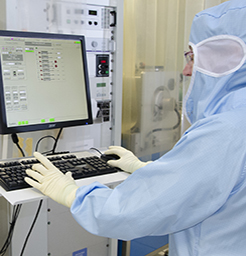
Working environment
  • The project will take place at the Institut d’Electronique, de Microélectronique et de Nanotechnologies (IEMN, https://www.iemn.fr/en/) which is a French major player in the field of micro/nanotechnologies and their
    applications. The IEMN is part of the INSIS institute of CNRS (http://www.cnrs.fr/index.php) and the Université de Lille (https://www.univ-lille.fr/), and located in the metropolitan area of Lille (110,000 students).
    The project will involve several research groups of the Nanostructured Materials and Components Department at IEMN. The main part of the project will be carried out in the Nanostructures, nanoComponents & Molecules (NCM, https://www.iemn.fr/la-recherche/les-groupes/groupe-ncm) group working in the physics of nanostructures and micro/nano-devices made of organic materials, self-assembled monolayers, oxide or iono-electronic materials. In addition, the project will benefit from the facilities available at IEMN such as (i) a multi-physics characterization platform (PCMP) and (ii) a clean room (ISO6 1600 m²). In particular, the candidate will work in the Pôle Microscopie en Champ Proche (PCP) which is one of the hubs of the PCMP platform. PCP brings together the means dedicated to the topographic, physical, and electrical analysis of surfaces from 100μm to the atomic scale such as STM, AFM, KPFM, etc. In summary, the facilities of IEMN cover all areas of micro and nanoelectronics from the elaboration and characterization of nanomaterials to their implementation into advanced nanodevices.
To apply :
Interested candidates are invited to send a CV, motivation letter and contact details of two referees to
Nataliya Kalashnyk
Junior Professor Chair
Tel: (+33) 03 20 19 79 07
E-mail: nataliya.kalashnyk@univ-lille.fr


Unité d’accueil :
IEMN UMR CNRS 8520
Avenue Poincaré
59652 VILLENEUVE D ASCQ CEDEX
www.iemn.fr

Date de début souhaitée :Octobre 2023

Durée souhaitée :1 an

Les candidatures accompagnées d’un CV et de 2 lettres de recommandation doivent être envoyées à :
Nataliya Kalashnyk

Junior Professor Chair
mailto:nataliya.kalashnyk@univ-lille.fr
tel : 03 20 19 79 07

Logo
Cité Scientifique
Avenue Henri Poincaré
CS 60069
59 652 Villeneuve d'Ascq Cedex, France
Tel : 03 20 19 79 79
CNRS Logo University of Lille Logo University Polytech Logo Junia Logo Centrale Lille Logo Renatech Logo RFnet Logo
Plan du site
© Copyright Service ECM et pôle SISR 2024
  • Production scientifique
  • Mentions légales
  • Politique de confidentialité
Faire défiler vers le haut
fr_FR
fr_FR
en_GB
Nous utilisons des cookies pour vous garantir la meilleure expérience sur notre site web. Si vous continuez à utiliser ce site, nous supposerons que vous en êtes satisfait.OKNonPolitique de confidentialité