

The reduction in size of semiconductor materials to the nanometer scale allows to restrict the degree of freedom of electron motion (or dimensionality) along 1, 2 or 3 directions in space. To date, due to growth constraints, the study of electron behavior has been limited to materials with strict dimensionalities (1D, 2D or 3D). An original study shows that materials obtained by colloidal chemistry processes can have a hybrid dimensionality, intermediate between 2D and 1D.
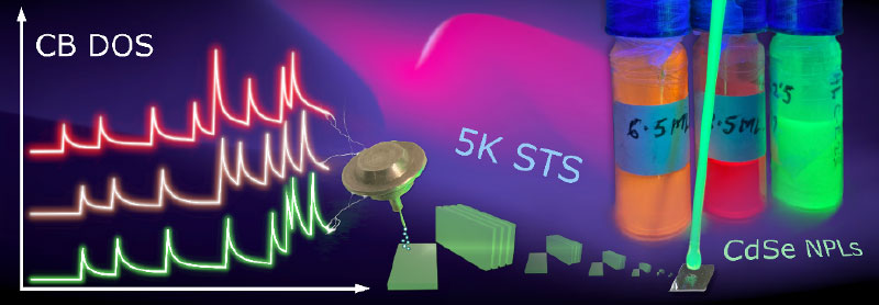
In massive materials, the properties of the charge carriers, i.e., the electrons, are directly derived from the materials themselves, independently of the external environment. However, this paradigm is no longer valid when these materials are reduced to the nanoscale. Indeed, at this scale, the degree of freedom of movement of electrons depends strongly on the size and shape of the materials. This strong dependence gives rise to spectacular effects such as the modification of the color of the light emitted by the same material by simply modifying its size as shown in figure 1. This color variation is associated with a modification of the electron energy induced by the quantum confinement. At the nanoscale, the degree of freedom of movement of electrons in materials, also called dimensionality (D), can be precisely controlled. Thus in carbon nanotubes, known as 1D, electrons can only propagate freely along the length of the tube.
The technological progress of the last twenty years has led to the development of standard materials allowing the exploration of electronic and optical properties associated with the different dimensionalities. Thus colloidal nanocrystals, carbon nanotubes, quantum wells obtained by epitaxy constitute the references for 0D, 1D, 2D dimensionalities respectively. At present, the different growth methods employed have not allowed to grow the materials in such a way as to explore continuously the dimensionality effects from bulk material to 0D nanostructures. Such studies require metrological control of the growth of the materials at the atomic layer scale in all three spatial directions.
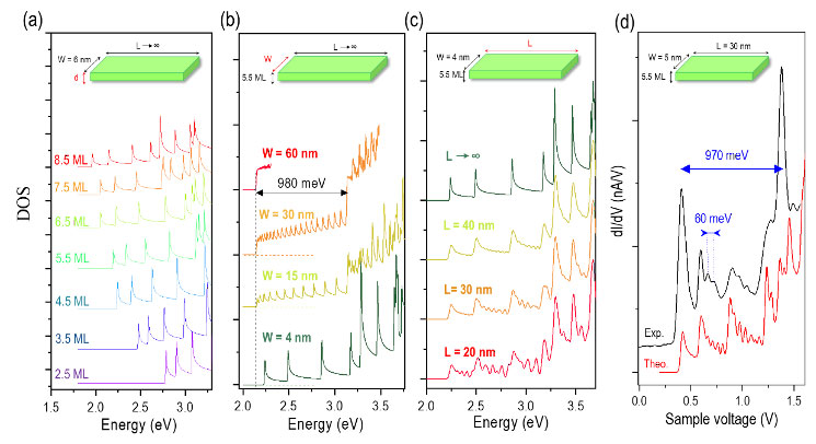
With this in mind, researchers from IEMN in collaboration with a team from the University of Ghent have shown that it is possible to obtain, by colloidal chemical synthesis processes, anisotropic CdSe nanoparticles, called NanoPlanets (NPLs), for which the electron confinement can be finely tuned in all 3 spatial directions. These NPLs exhibit strong quantum confinement depending on their thickness which is in the nanometer range and is controlled to the nearest atomic layer. The lateral dimensions can be varied from a few nanometers to a hundred nanometers which allows to modify the electron confinement and to study finite size effects. Tunneling microscopy studies have shown that, for NPLs with finite lateral dimensions smaller than 30 nm, the densities of electronic states show Van Hove singularities, characteristic of 1D materials, in very good quantitative agreement with theoretical calculations of strong bonds, and in clear contradiction with the paradigm widely accepted for a decade for NPLs, of a 2D density of state for electrons in the conduction band.
These first results published in Nanoletters1 pave the way towards an understanding of the electronic properties at the dimensional boundary, which is essential for the development of functional hetero-nanostructures that would use the inherent advantages of different dimensionalities to optimize performance.
(1) Peric, N.; Lambert, Y.; Singh, S.; Khan, A. H.; Vergel, N. A. F.; Deresmes, D.; Berthe, M.; Hens, Z.; Moreels, I.; Delerue, C.; Grandidier B.; Biadala L. Van Hove Singularities and Trap States in Two-Dimensional CdSe Nanoplatelets. Nano Lett. 2021, 21 (4), 1702–1708. https://doi.org/10.1021/acs.nanolett.0c04509.


