IEMN
  • Accueil
  • Actualités
    • Newsletters de l’IEMN
    • Offres de Stages M2-Ingé
    • Les offres d’emplois
    • Toutes les actualités
  • L’Institut
    • Présentation
    • Organisation de l’institut
    • La Direction Scientifique
    • La Direction Technologique
    • La direction administrative et financière
    • Règlement intérieur
    • Nos engagements
  • La Recherche
    • Les départements scientifiques
      • Matériaux Nanostructures et Composants
      • Micro/nano et optoélectronique
      • Technologies des télécommunications et Systèmes intelligents
      • Acoustique
    • Les groupes de recherche
    • Les projets phares
  • Production Scientifique
    • Publications IEMN
    • Ressources production scientifique
  • Les plateformes
    • CMNF – Plateforme Centrale de Micro Nano Fabrication
      • Pôle Gravure et implantation
      • Pôle Analyse In Line
      • Pôle Soft Lithographie et Bio Microfluidique
      • Pôle Dépôts et épitaxie
      • Pôle Lithographie
      • Pôle Packaging
      • Staff CMNF
    • PCMP – Plateforme de Caractérisation Multi-Physique
      • Pôle Microscopie en Champ Proche (PCP)
      • Pôle Caractérisation Hyperfréquence, Optique et Photonique (CHOP)
      • Pôle Systèmes de COMmunications avancées et prototypage (SigmaCOM)
      • Pôle Caractérisation et Compatibilité ElectroMagnétique et prototypage (C2EM)
      • Staff PCMP
    • Prestations proposées par nos plateformes
  • Partenariat – Valorisation
    • Les Collaborations Académiques
    • Projets ANR
    • Principales collaborations internationales
    • Les partenariats industriels
    • Les laboratoires communs IEMN-Industrie
    • Les startups
  • La Formation à la Recherche
    • L’après-thèse
      • Faire un post-doc à l’IEMN
      • Vers le monde des entreprises et de l’industrie
      • Devenir Enseignant-Chercheur
      • Devenir Chercheur
      • Créer son entreprise à l’IEMN
      • FOCUS sur un ingénieur SATT issu de l’IEMN
    • Une thèse à l’IEMN
      • Soutenances de thèses et HDR
      • Sujets de thèses
      • Les financements
      • Les études doctorales
    • Master – Ingénieur
      • Masters ULille
        • Master Life Sciences and Technologies graduate program
        • Master Nanosciences and Nanotechnologies – Speciality ETECH
        • Master Réseaux et Télécommunications
      • Masters UPHF-INSA
        • Master Ingénierie des Systèmes embarqués et Communications Mobiles
        • Master Cyber-Défense et Sécurité de l’information
        • Master Matériaux, Contrôle, Sécurité
        • Master Ingénierie des Systèmes Images et Sons
      • Écoles Ingé partenaires/tutelles
      • Offres de Stages M2-Ingé
    • Le pôle lillois du GIP-CNFM
    • Nano-École Lille
  • Contact
    • Localisation
    • Formulaire de contact
    • Annuaire Intranet
  • Nos soutiens
  • en_GB
  • Rechercher
  • Menu Menu
ACTUALITES

2D materials: beyond graphene…

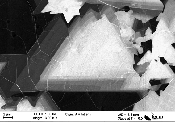
Fig. 1: growth of hBN under ultra-high vacuum, formation of triangular domains of several aligned planes

  • hBN: the best ally of graphene

Graphene is a material famous for its exceptional electronic properties.
However, if these properties are to be exploited in real components, it is essential to reduce electronic interaction with the environment as much as possible. Hexagonal boron nitride (hBN), another 2D material characterized by a very wide band gap (~6 eV), is very promising for this purpose. It can be used both to isolate graphene from the substrate and as a gate dielectric material. The study of the growth of hBN by molecular beam epitaxy started at IEMN in 2017 (see figure 1), in an ultra-high vacuum growth chamber that also allows the growth of graphene.

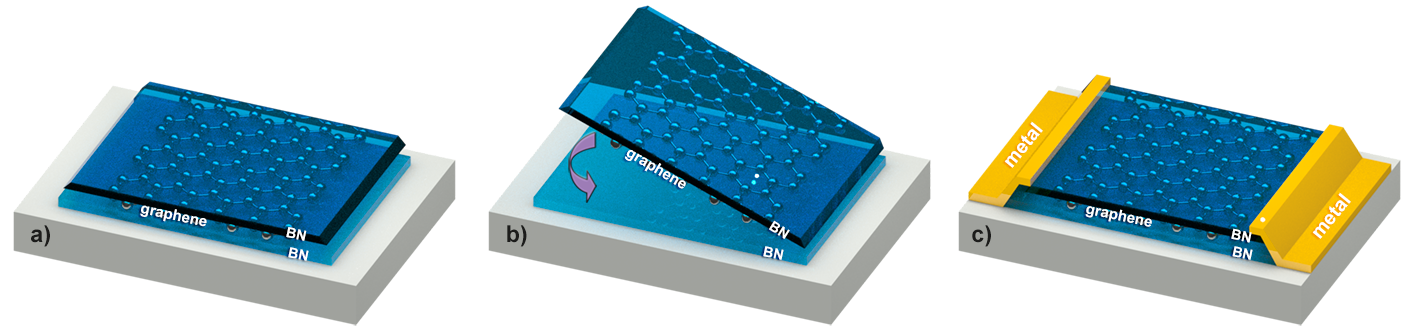
Fig.  2: 2DHetero project, a) complete heterostructure obtained by growth,
b) heterostructure requiring a transfer step and c) test component

The first results have notably led to the 2DHetero project, which has just been selected in the framework of the Flag-Era 2019 call. The aim of this project is to explore the direct growth of complete hBN/graphene/HBN heterostructures using coupled molecular beam epitaxy and chemical vapor deposition techniques (see figure 2a), avoiding as much as possible any transfer/report step of a part of the heterostructure (figure 2b). IHP Frankfurt/Oder (Germany) and the University of Namur are the other members of the 2DHetero consortium.

  • And with a forbidden band…

For more than fifteen years, the exceptional properties of graphene have stimulated materials research and led to numerous proposals for applications. Nevertheless, the absence of band gap remains an obstacle to the use of graphene in many micro and optoelectronic devices and thus to the development of 2D electronics. Other 2D materials and among them transition metal dichalcogenides (DMTs), with a band gap of 1 to 2 eV, can then take over. These materials offer properties that are not found in usual semiconductors: absence of hanging surface bonds, nature of the band gap varying with thickness, strong optical absorption, valleytronics,… It is in this perspective that to develop its activity on 2D materials, the IEMN has equipped itself at the beginning of 2020 with a frame for molecular jet epitaxy (MJE) of heterostructures of DMTs. This Vinci Technologies system is connected under ultra-high vacuum to a surface analysis chamber and a III-V semiconductor EJM frame. It is equipped with a valve cracker cell as Selenium source and a 6-crucible electron gun and Knudsen effusion cells for metal evaporation. It will be dedicated to the epitaxy of DMT heterostructures but also to the growth of hybrid III-V/2Ds heterostructures.

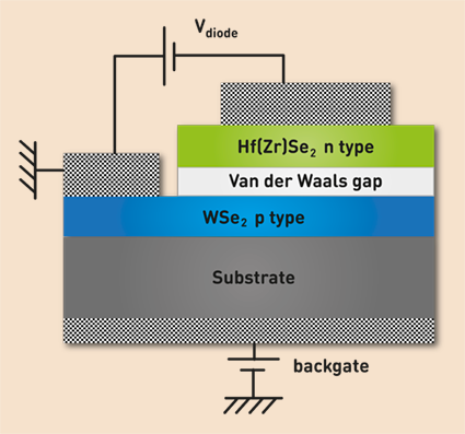
Fig. 3: Example of DMT heterostructure
for the realization of Esaki diodes

Logo
Cité Scientifique
Avenue Henri Poincaré
CS 60069
59 652 Villeneuve d'Ascq Cedex, France
Tel : 03 20 19 79 79
CNRS Logo University of Lille Logo University Polytech Logo Junia Logo Centrale Lille Logo Renatech Logo RFnet Logo
Plan du site
© Copyright Service ECM et pôle SISR 2024
  • Production scientifique
  • Mentions légales
  • Politique de confidentialité
Faire défiler vers le haut
fr_FR
fr_FR
en_GB
Nous utilisons des cookies pour vous garantir la meilleure expérience sur notre site web. Si vous continuez à utiliser ce site, nous supposerons que vous en êtes satisfait.OKNonPolitique de confidentialité