08/11/2019
10h30 – IEMN Laboratoire Central – Salle du conseil
Campus Cité Scientifique – Villeneuve d’AscqProf. Aitor MUGARZA
Catalan Institute of Nanoscience and Nanotechnology – Bellaterra (Barcelona)
« Atomic Manipulation and Spectroscopy » group leaderhttps://icn2.cat/en/atomic-manipulation-and-spectroscopy-group/aitor-mugarza
Abstract :
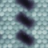
 Nanostructuring graphene confers multiple functionalities to this material, making it attractive to very diverse applications in electronics, molecular sensing and filtering. For instance, semiconducting gaps can be induced by reducing its dimensions to the nanometer scale, whereas introducing pores of similar sizes turns impermeable graphene into the most efficient molecular sieve membrane. In both cases, the interesting scale for applications is below 3-5 nm, a regime where bottom-up synthesis can be particularly efficient.
Here I report different on-surface methods to grow graphene quantum dots with controlled shape and edge structure [1], periodic arrays of nanoribbons with lengths exceeding 100 nm [2,3], and nanoporous graphene sheets that combine 1nm size ribbons and pores [4]. Their novel electronic states are correlated with the particular atomic structures by using STM. Their potential application in devices is illustrated by gate modulated transport measurements in nanoporous graphene sheets.
[1] S. O. Parreiras et al., 2D Mater., 4 25104 (2017).
[2] C. Moreno et al., Chem. Commun. 54, 9402 (2018).
[3] C. Moreno et al., Chem. Mater. 31, 331–341 (2019)
[4] C. Moreno et al, Science (80-. ). 360, 199 (2018).


