Ali ABBOUD
« Development and optimization of technological process to fabricate
active devices on wide band gap semiconductors »
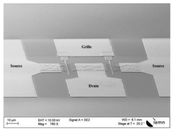
SEM view of a High Electron Mobility Transistor with short gate-length
My mission as engineer within the group is to develop active devices dedicated to high frequency / high power applications in clean room. These devices (specifically High Electron Mobility Transistors) are based on wide bandgap semiconductors such as GaN, AlGaN, AlN.
I am in charge of the adaptation of a well established process to fabricate GaN based HEMTs on different substrates (Si, SiC or GaN) taking into account the barrier material (AlGaN, In AlN, AlN) of the heterostructure. The fabrication of these devices requires different technological process steps such as ohmic contacts, devices isolation, gate contacts, passivation. Thus, I use all the equipment available in clean-room (optical and e-beam lithography equipements, etching equipments, evaporation, …). In addition, intermediate characterizations are performed to validate the different steps of the process (TLM and HALL Measurements).


